Measuring devices
for the field of application
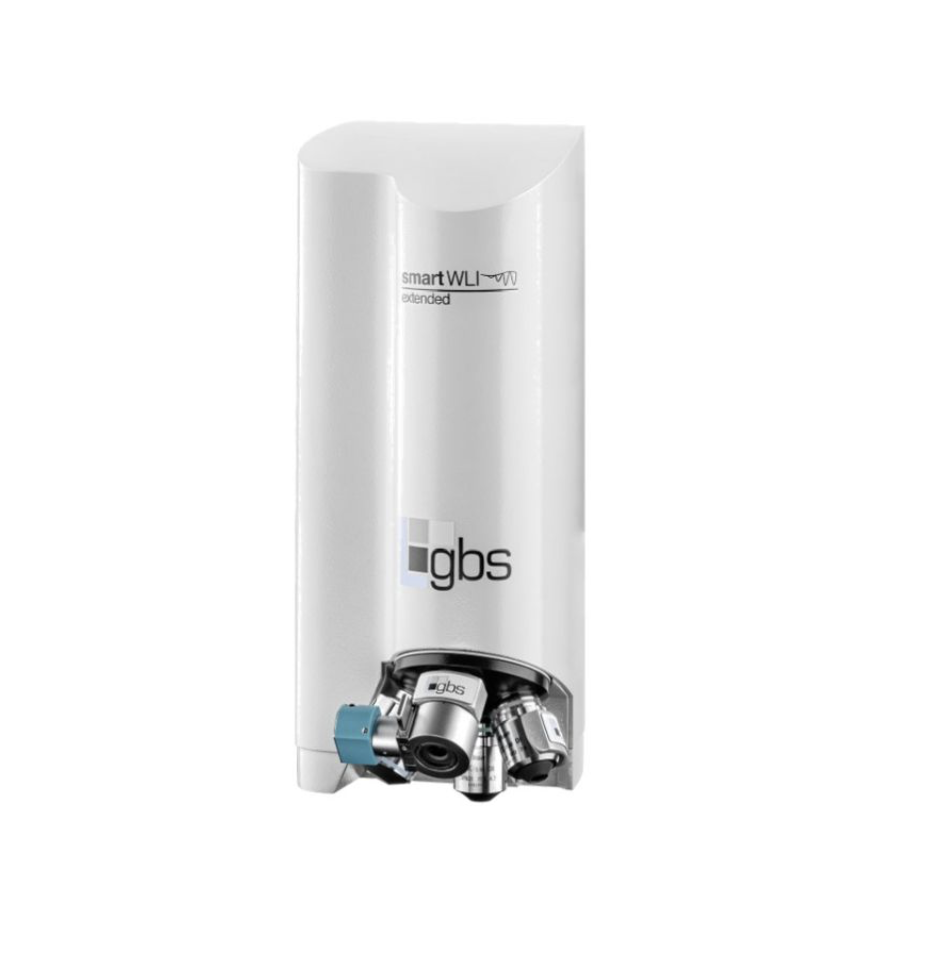
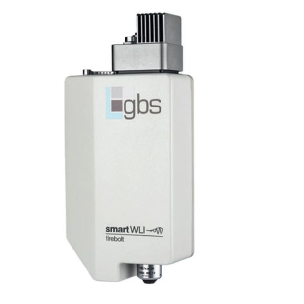
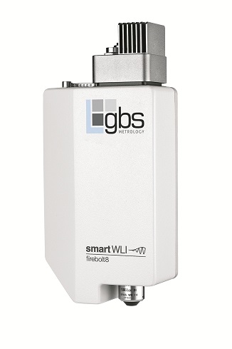
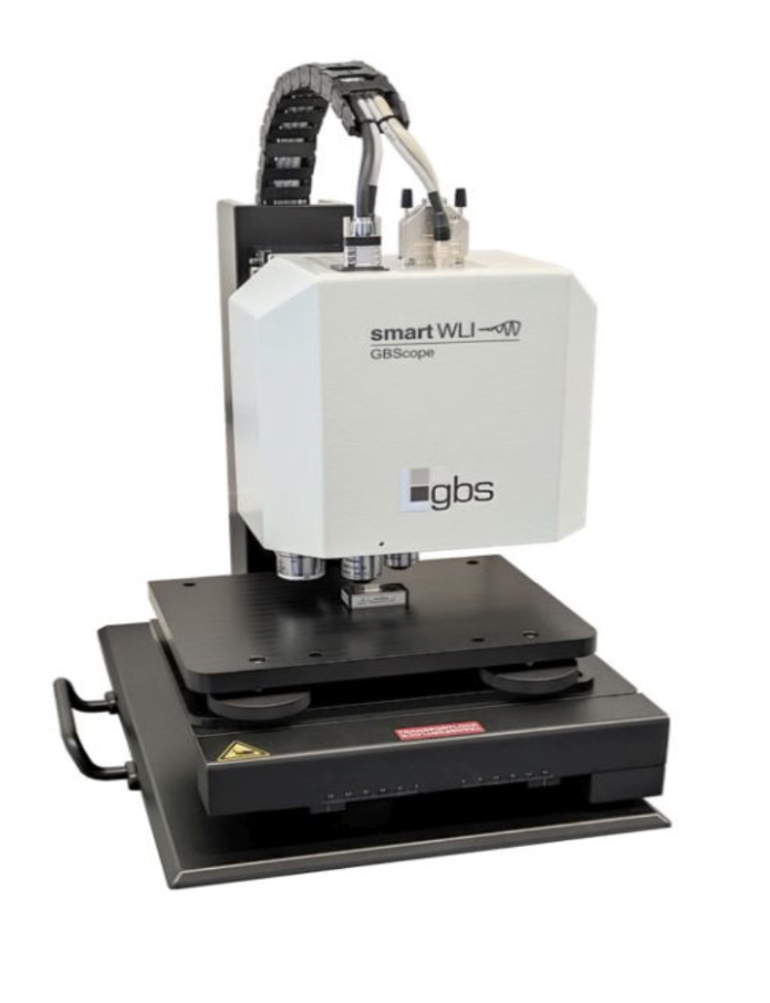
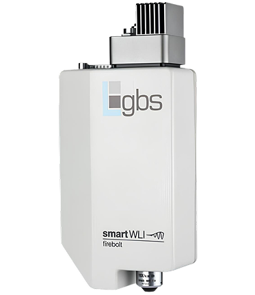
production & integration
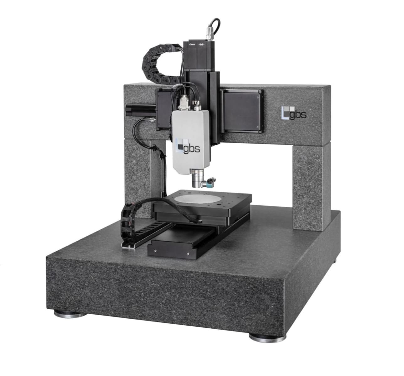
Designed for use in production and directly in manufacturing processes, our measuring devices are characterized by their robustness, short measuring times, and easy integration into existing production lines. They support efficient quality assurance with fast, non-contact measurements—both inline and close to production—and are specially tailored to the requirements of industrial applications.


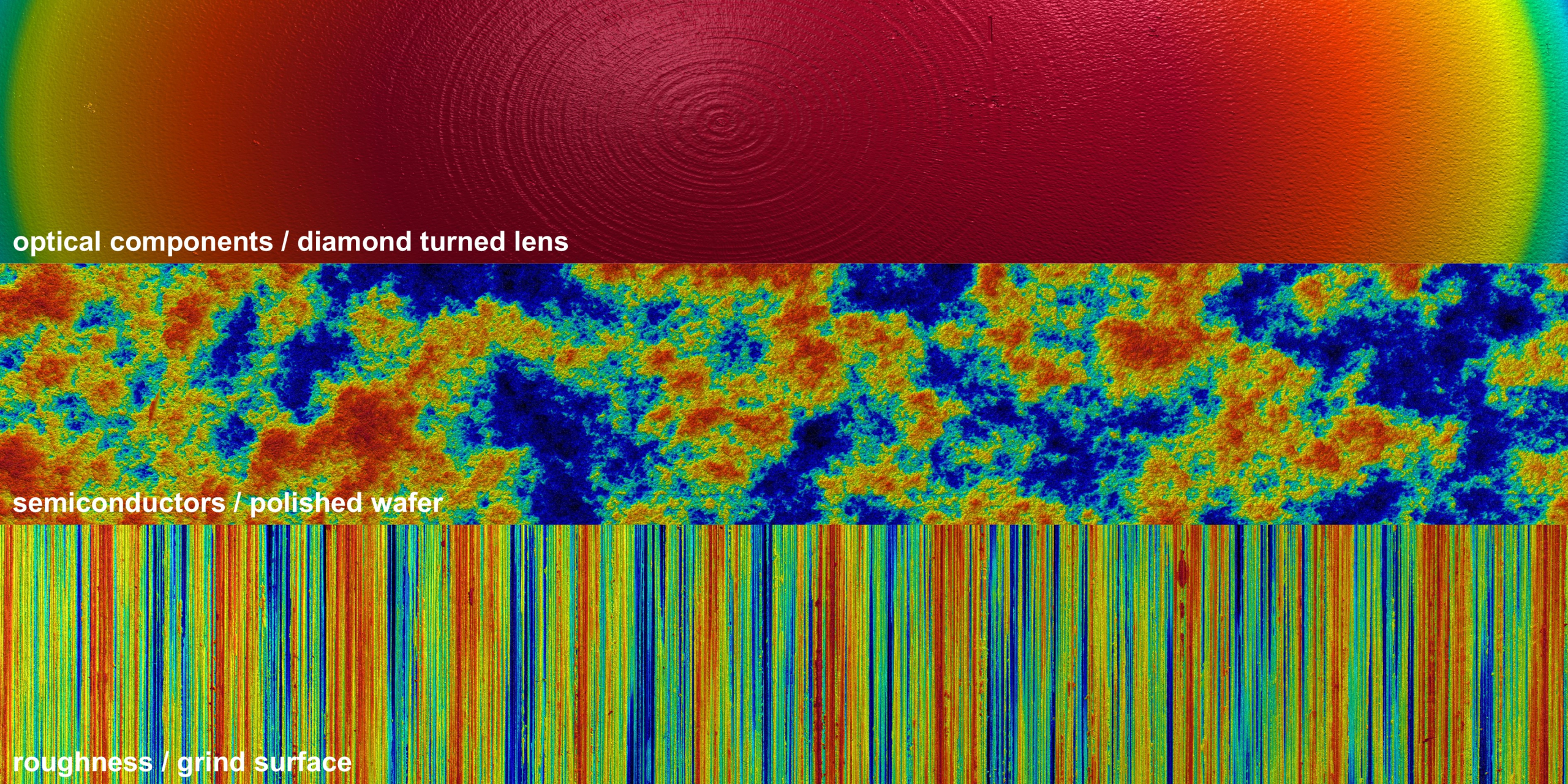
Use of Coherence Scanning Interferometry (White Light) for the measurement of surface roughness and micro-geometries
Coherence scanning (white-light) interferometry offers significantly higher resolution than competing optical 3D measurement techniques such as confocal microscopy, focus variation, chromatic confocal sensors, fringe projection, or laser triangulation sensors.
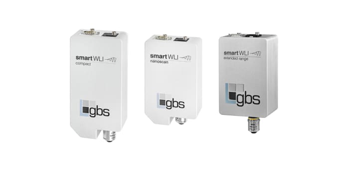
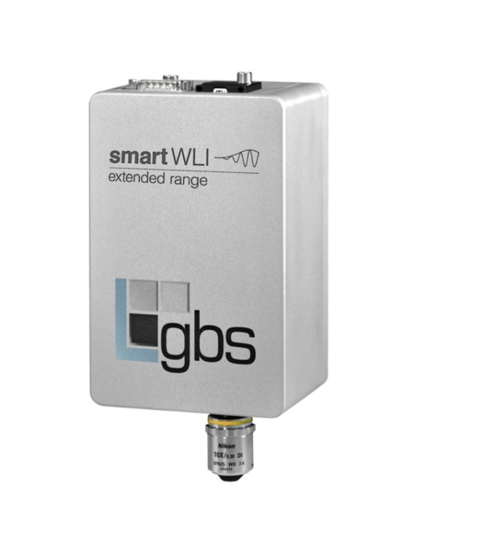
Advantages of smartWLI sensors and optical profilers compared to other coherence scanning (white-light) interferometers
High-speed cameras combined with massively parallel data processing accelerate both data acquisition and evaluation processes, making the systems more robust and less sensitive to vibrations.
This speed enables the acquisition and stitching of several hundred individual scans, even under challenging conditions.
Individual scans with typical cycle times of 1 to 3 seconds per scan.
Data processing, including contrast enhancement, model-based signal correction, and data quality monitoring, enables the reliable detection of weak signals in steeply inclined areas.
Precise 3D surface
metrology for every application
Our optical measurement solutions cover the entire spectrum of 3D surface analysis—from high-precision devices for laboratories and research to robust systems for production and integration to custom-developed special solutions. Whether you need to measure micro- and nanostructures or roughness, you will receive the optimal non-contact measurement technology for every application—reliable, flexible, and tailored precisely to your requirements.
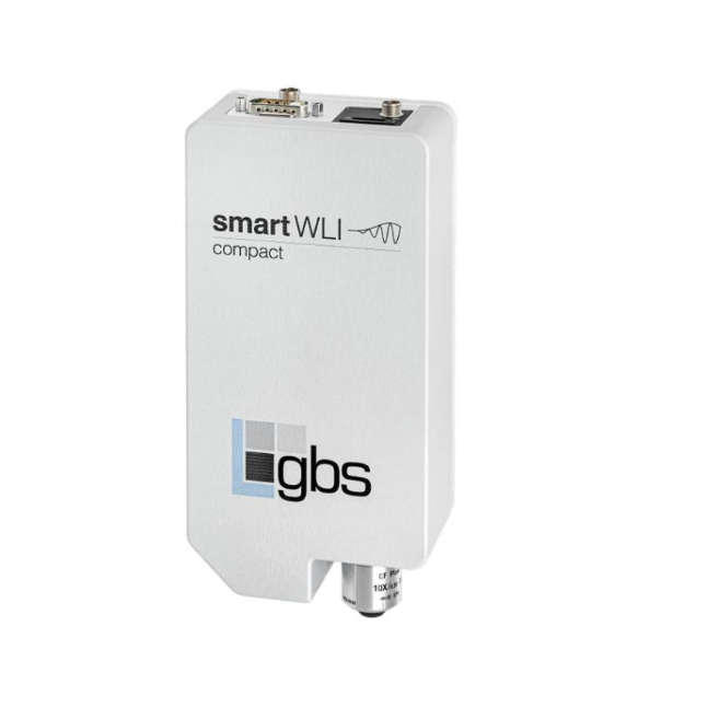
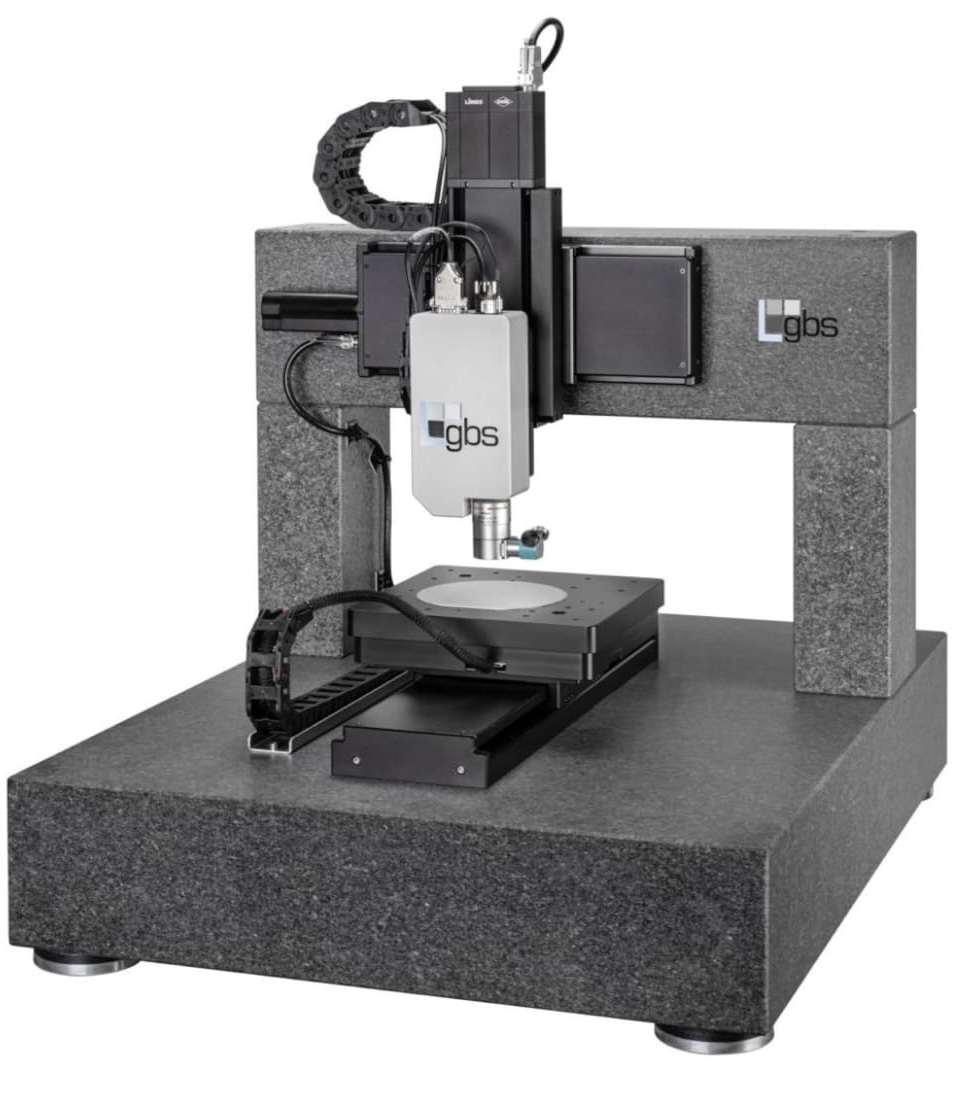
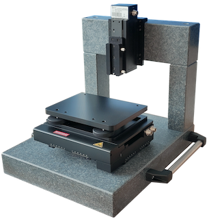
Measuring instruments for laboratory and research applications
Our measuring devices for laboratories and research are specially designed for maximum precision and flexibility. They enable detailed analyses of micro- and nanostructures and deliver reliable measurement results for demanding research and development projects. With state-of-the-art white light interferometry and innovative image processing, these systems offer ideal conditions for scientific applications and technical quality management.
Customized solutions
Every product is only as good as its fit – that’s why we develop individual, customer-specific metrology solutions that are precisely tailored to your requirements and processes. Whether you need custom-made products, adaptations to existing systems, or complex measuring stations, our experienced team will support you from the design stage through to commissioning and beyond.
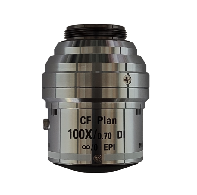
Discover our accessories
Modern 3D surface measurement technology requires powerful software—both for the precise control of the measuring systems and for the detailed evaluation of the recorded data. Our software solutions form the perfect combination of hardware, ease of use, and analytical depth.
Why GBS?
We measure, analyze, and visualize technical surfaces in 3D—from tool steel to semiconductor wafers. Precise. Comparable. Reproducible.
Years of market experience
industrial partners
Made in Germany
systems installed in the last 5 years
Our advantages
GBS metrology GmbH offers advanced optical 3D metrology that perfectly combines precision, reliability, and efficiency. Our non-contact systems for roughness, microstructure, and nanostructure measurements deliver reproducible results, save testing time, and can be flexibly adapted to your individual requirements—ideal for research, development, and modern manufacturing.
In-house product development
Minimal maintenance required
Full automation possible
Faster ROI of products
First-hand support
Short measurement times – real-time evaluation on GPGPUs