Microsystem technology: Precise measurements for the highest demands
In microsystem technology, tiny structures meet maximum functional density — and the demands on measurement technology are correspondingly high. Our 3D surface measurement technology enables precise, non-contact characterization of microstructured components in all development and manufacturing phases.

GBS metrology GmbH: Precision in surface measuring technology
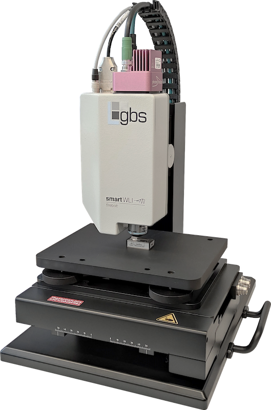
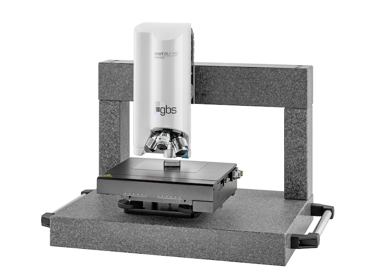
Since 1997, GBS metrology GmbH has been developing, manufacturing, and distributing high-precision measuring technology for analyzing microgeometries, surface structures, and roughness. The product portfolio includes optical 3D sensors, profilometers, gantry measuring devices, and production-oriented measuring stations.
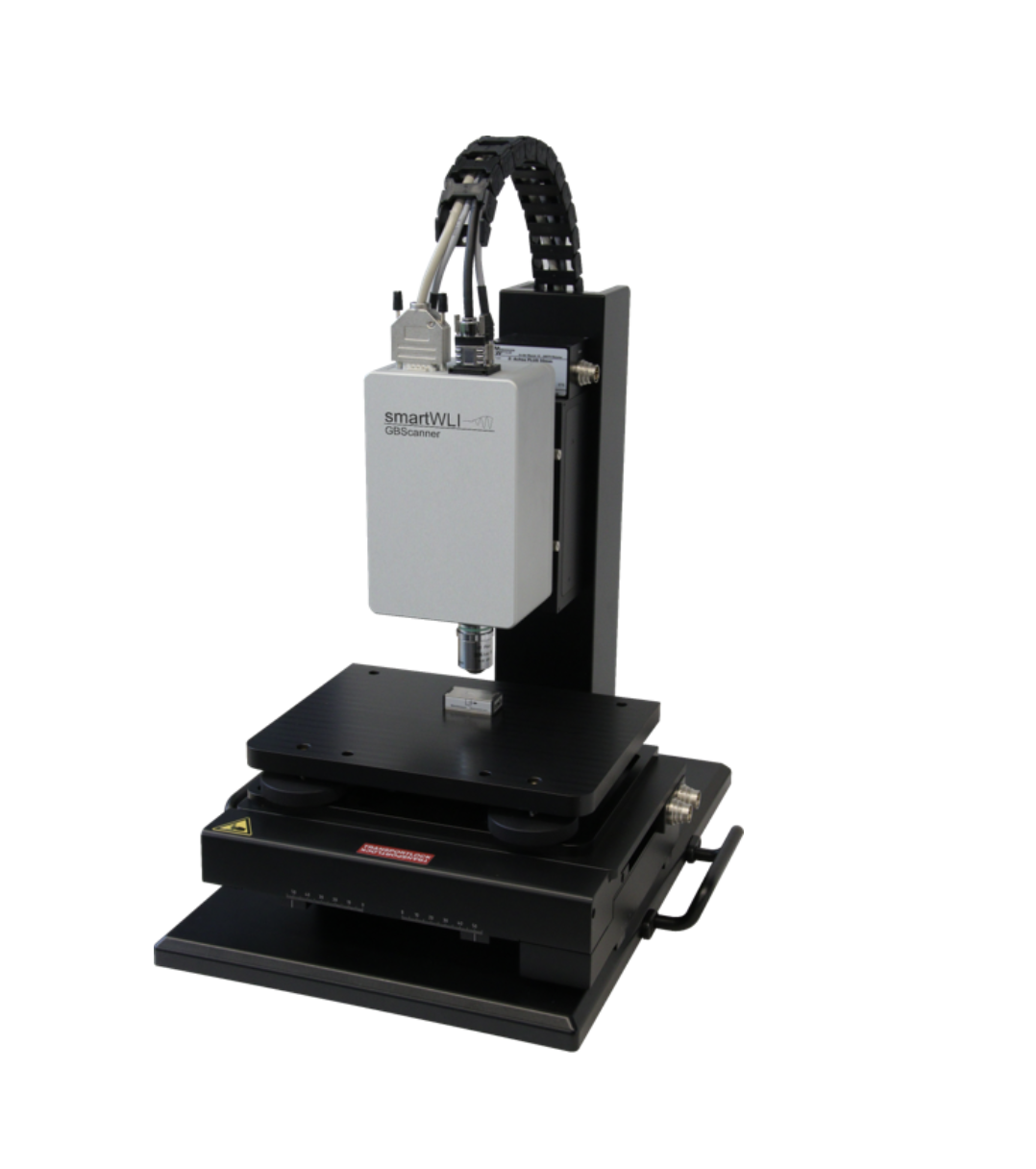
Thanks to parallel image processing on powerful GPGPU systems, the measuring devices can be used in laboratories, in production, and inline. The white light interferometry used enables the high-resolution measurement of a wide variety of surfaces. The “smartWLI” product line stands for innovative 3D surface measurement technology in the micro and nanometer range.
3D surface measurement technology for microsystems: applications and functions
Development and testing of MEMS
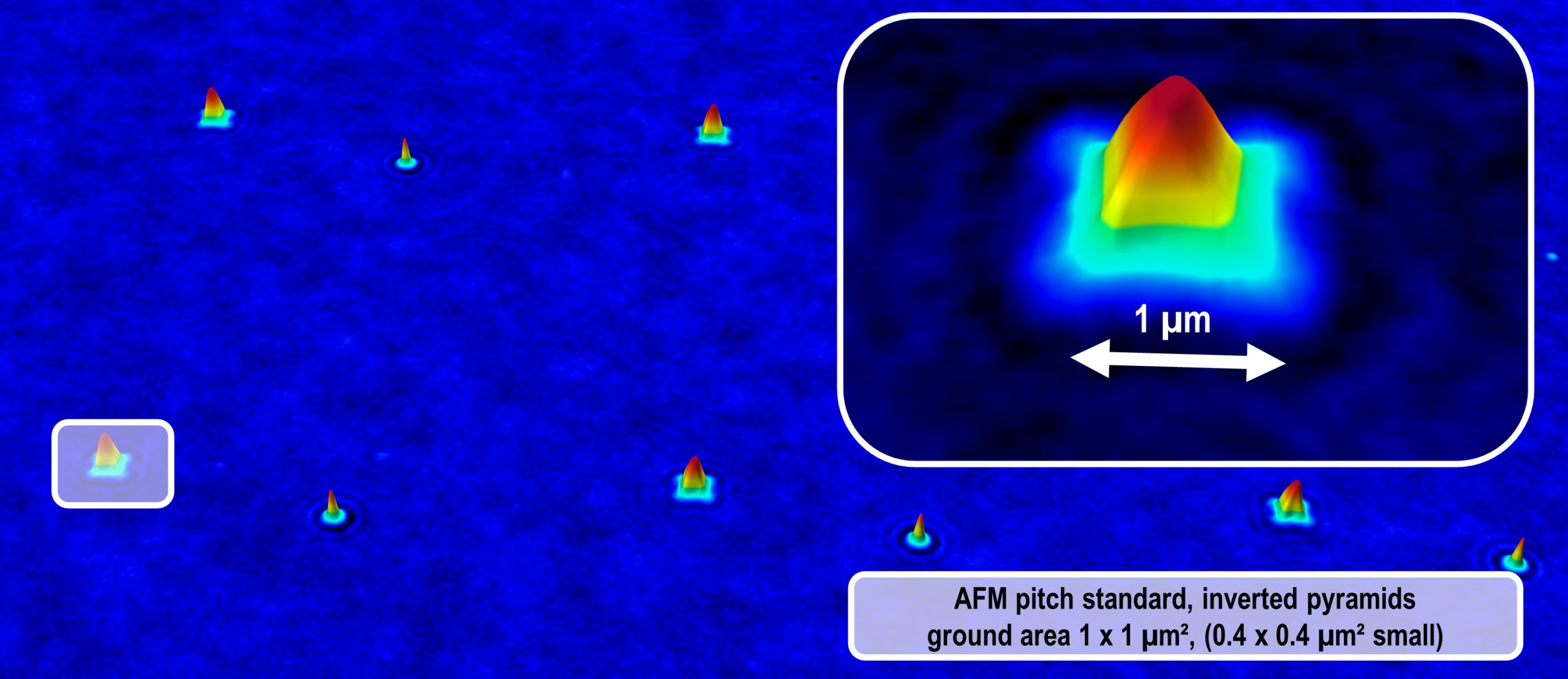
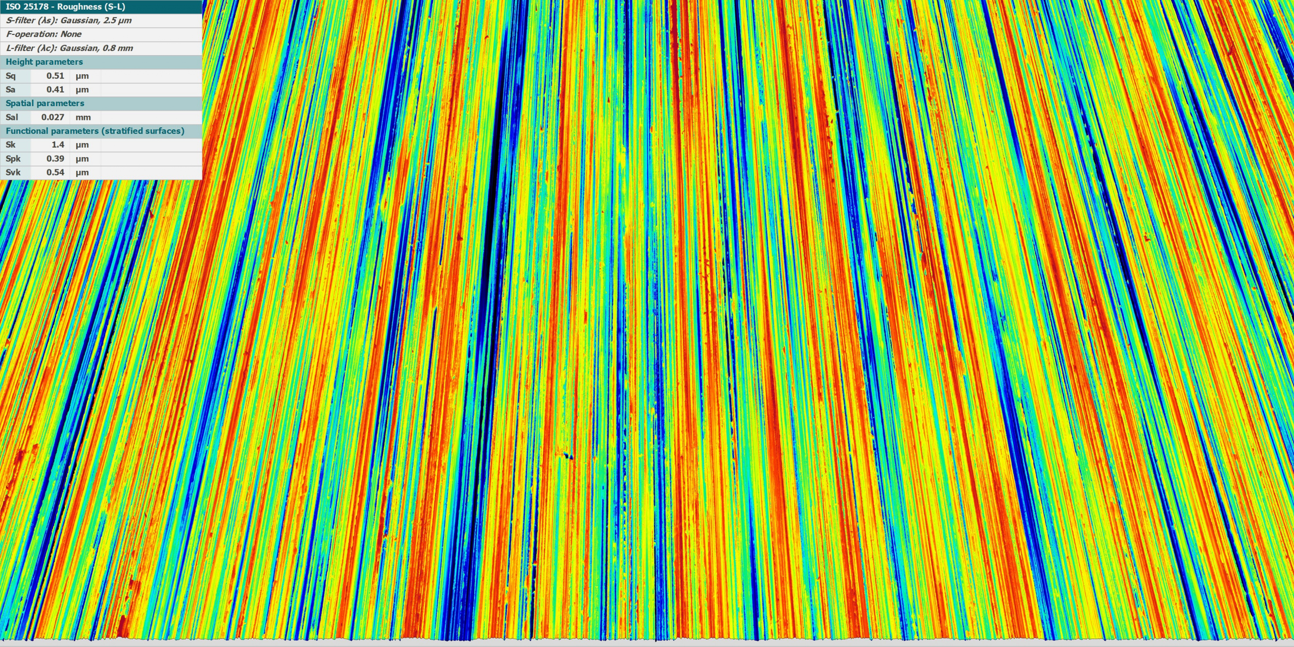
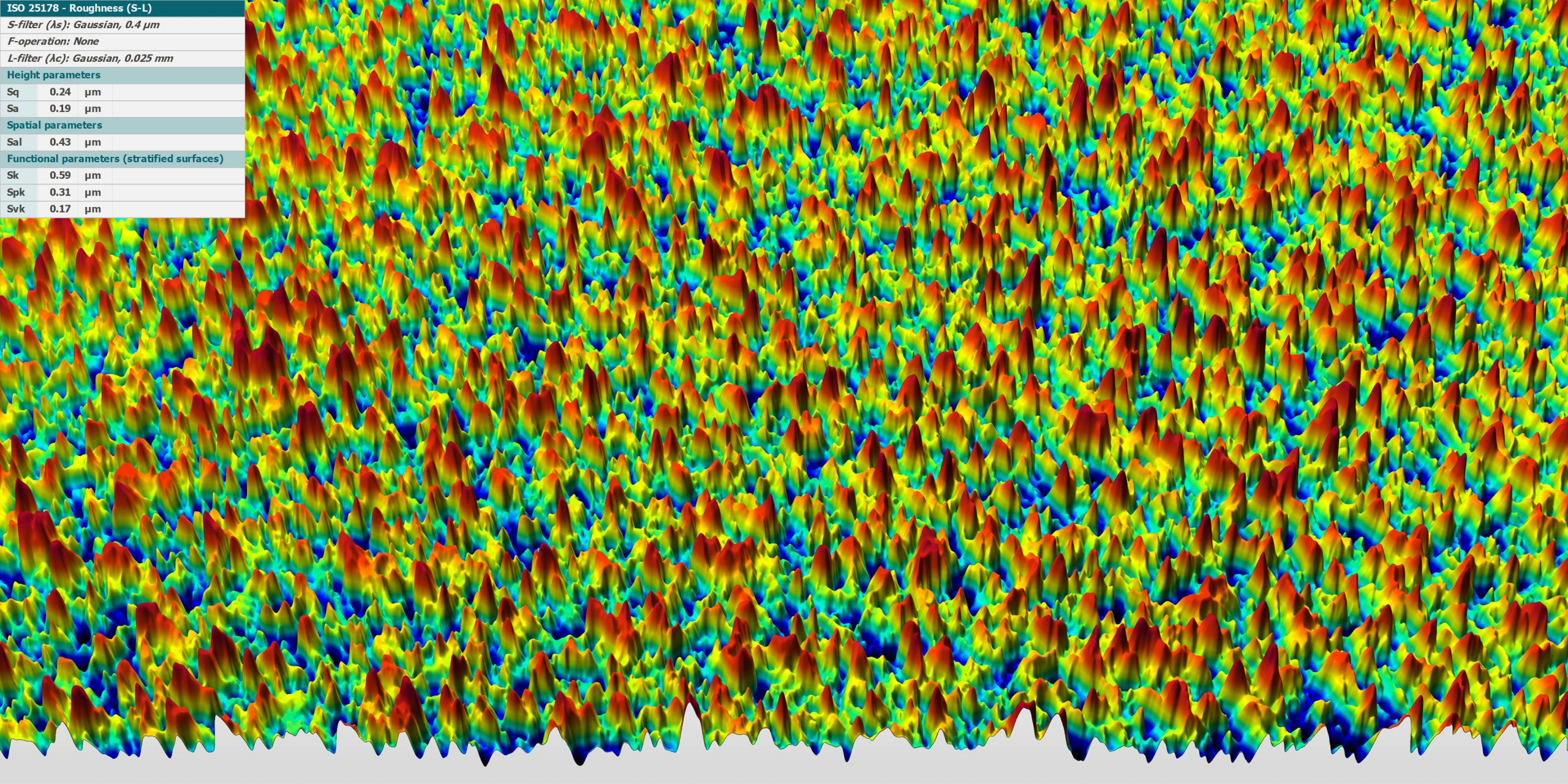
Microsystem technology involves the manufacture of MEMS components with complex structures. GBS’s 3D surface measurement technology analyzes topography, roughness, and dimensional accuracy to ensure functionality and reliability.
Measuring microfluidic channels
In microfluidic systems, channels and transitions are precisely measured. The measuring systems determine cross-section, flatness, and surface roughness from the micrometer to the nano- and sub-nanometer range.
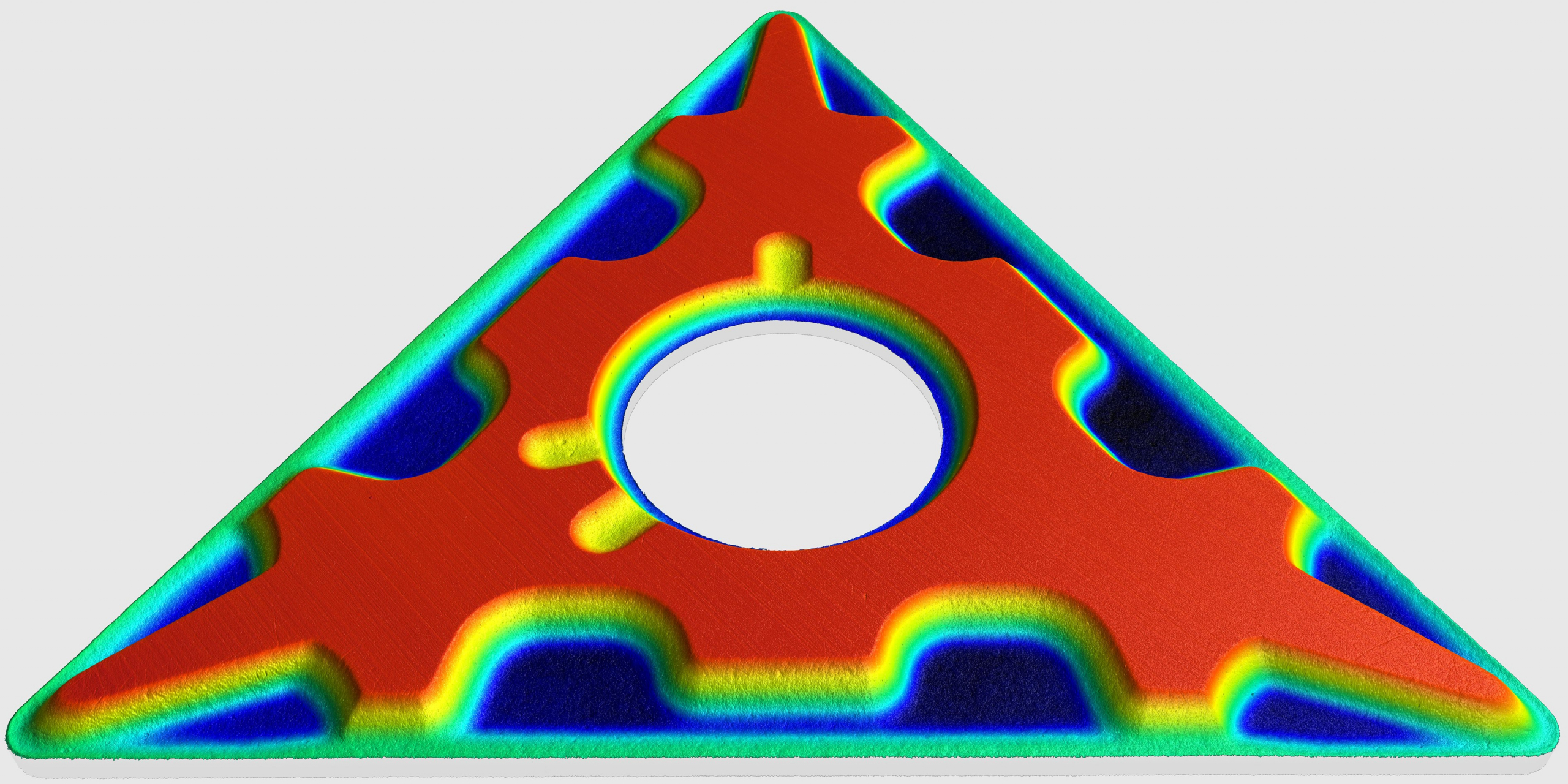
Inspection of micro-optics
The quality of micro-optics depends largely on flatness, curvature, and surface quality. Optical 3D measurement technology documents these parameters without contact and in great detail.
Inline monitoring of sensor production
During the production of microstructured sensors, inline measurement technology enables continuous monitoring of geometry and surface structure to ensure process stability.
Defect detection in microstructured components
Defects such as particles, scratches, or local structural deviations are detected at an early stage. This allows faulty components to be identified and sources of error to be analyzed.
Final inspection and quality documentation
Before delivery or further processing, microstructured components undergo a final inspection. 3D surface measurement technology provides documented measurement values to ensure production standards are met.
Technological features and advantages of GBS measuring systems for microsystem technology
GBS measuring systems for microsystem technology are based on coherence scanning interferometry and use massive parallel image processing with GPGPU technology. This combination enables high-speed, high-resolution measurements, allowing even complex microstructured surfaces to be reliably captured.
The systems are designed for inline use and automation and can be easily integrated into production lines. Advanced evaluation ensures the differentiation of critical structural details and delivers reproducible measurement results.
Companies benefit from non-contact and non-destructive analysis that does not affect even sensitive components. Fast measurement data acquisition supports high cycle times in production and allows flexible adaptation to different measurement tasks.
All measurement results are documented and traceable, enabling seamless quality assurance and effective process optimization. GBS systems are suitable for both development tasks and series production of microsystems.
The advantages of our 3D surface measurement technology
- Non-contact and non-destructive measurement of sensitive microstructures
- High resolution down to the sub-nanometer range
- Fast and reproducible data acquisition for process and quality control
- Can be automated and integrated inline into production lines
- Flexible adaptation to different component sizes and measurement tasks
- Complete documentation and traceability of all measurement results
Precise measurements in microsystems technology
GBS offers powerful optical 3D measurement systems that have been specially developed for the requirements of microsystems technology. The measurement systems enable non-contact, high-resolution analysis of micro- and nanostructures in all development and manufacturing phases. Companies benefit from automatable solutions that can be flexibly integrated into existing processes.
Automation and integration into production
The integration of GBS’s 3D surface measurement technology into production enables automated and continuous quality monitoring of microstructured components. Thanks to modern interfaces and powerful software, the measurement systems can be integrated directly into production lines and linked to existing automation solutions.
This allows measurements to be taken in real time and results to be evaluated immediately. Production processes become more efficient as errors are detected early on and scrap is minimized. The systems can be configured flexibly and easily adapted to different component types or changing production requirements.
Real-time measurements enable deviations or errors to be detected immediately during production. Immediate evaluation of the measurement data allows for rapid process adjustments, effectively reducing scrap.
Our product highlights


What our customers say

Measuring stations for rapid testing of precision turned parts in the production environment
At the start of each shift, the dimensional accuracy of the turning tools is checked in the precision turned parts production department at Klumpp Präzisionswerk GmbH & Co. KG. To this end, workpieces from ongoing production are sent to the measuring laboratory to obtain approval for further production. In series production with multiple automatic lathes, however, the large number of measurements often leads to the laboratory becoming overloaded.
GBS metrology GmbH developed an automated measuring station. The measuring station can be installed directly in the production environment, close to the lathes. This allows workers to check their finished products themselves without any prior knowledge of measurement technology or training.
After installing the measuring station from GBS metrology, it was quickly integrated into the production process and was very well received. The reduction in personnel required in the measuring laboratory and the resulting acceleration of production approval led to a clear increase in the scope and efficiency of the manufacturing processes.
FAQ
Our systems can precisely measure structures with a lateral size of approximately 0.3 micrometers or greater. Even the smallest details in the nanometer range are captured contactlessly and reproducibly.
The measuring systems are designed for integration into automated production environments. Thanks to modern interfaces and software, they can be flexibly and seamlessly integrated into existing production processes.
A wide variety of micro- and nanostructured surfaces can be analyzed, such as MEMS, sensors, micro-optics, and microfluidic systems. Even sensitive and complexly structured components can be reliably measured.