Optical 3D Sensors: Advantages and Applications
- 3D sensors capture surface structures precisely and contactlessly.
- High resolution and rapid data evaluation are enabled by GPGPU technology.
- Versatile applications include manufacturing, semiconductors, medical technology, and research.
- Flexible integration into production lines and laboratories is possible.
- Practical examples demonstrate benefits in quality assurance and product development.
The demands on manufacturing and research are continually increasing. Capturing and evaluating surface structures, micro- and nano-geometries, and roughness is becoming ever more complex.
Modern 3D sensors are designed for these tasks, enabling efficient, reliable, and detailed surface analysis through optical measurement methods. This article explains how 3D sensors work, their advantages, and the areas in which they are applied.
What Are Optical 3D Sensors?
Optical 3D sensors are measurement systems that capture surface structures and micro-geometries contactlessly and in three dimensions. Unlike tactile systems such as probes or conventional profilometers, these sensors use light and specialized algorithms to obtain precise height and structural data.
Modern devices often employ white-light interferometry, where height information is calculated by analyzing interference patterns. Data processing is performed on powerful graphics processors (GPGPU), allowing large image datasets to be analyzed in real time. This makes optical 3D sensors suitable not only for laboratory use but also for integration into production processes.
Advantages of Optical 3D Sensors
Compared to other measurement methods, optical 3D sensors provide high resolution in height and surface measurements. Their contactless operation prevents damage to sensitive samples and allows measurement of soft or flexible materials.
High-speed data acquisition enables inline monitoring in production lines. Using GPGPU technology, measurement data is processed without delay, allowing cycle times of 1 to 3 seconds per measurement. Advanced quality control algorithms check each measurement signal and eliminate outliers, increasing the reliability of results.
The sensors are robustly built and suitable for integration into automated systems. With various objectives and a modular design, the systems can be flexibly adapted to different measurement tasks.
Key Advantages:
-
Contactless and fast measurement, even for sensitive or large workpieces
-
High resolution and real-time processing through modern data handling
-
Flexible adaptation to various applications and easy integration into production lines
-
Reliable results through advanced quality control
Applications of Optical 3D Sensors
Quality Assurance in Manufacturing
3D sensors are integrated directly into production lines to continuously monitor surface features. Their fast measurement and real-time evaluation make them ideal for automated quality control in machining processes, such as checking roughness values and microstructures.
Surface and Roughness Analysis
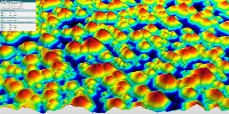
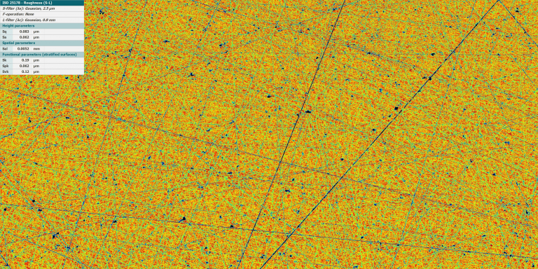
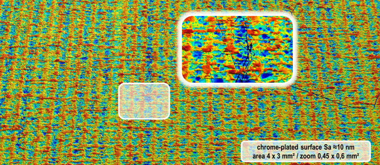
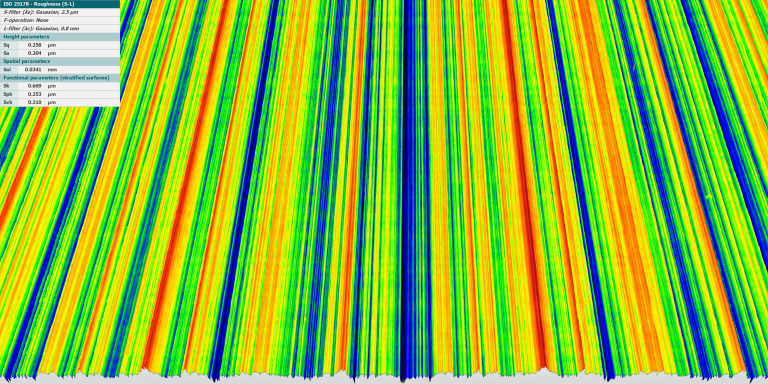
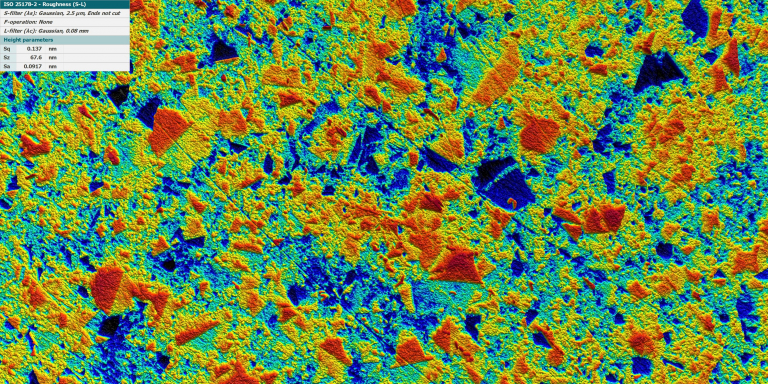
In the automotive and supplier industry, 3D sensors are standard for evaluating ground, polished, or finished metal surfaces. They also provide detailed data on roughness, bearing area curves, and nanostructures for additively manufactured components.
Semiconductor and Electronics Manufacturing
Optical sensors are used to inspect wafer surfaces, measure solder points, and examine microlens arrays. Even the smallest defects are reliably detected. Measurements on polished and structured wafers often require objectives with up to 115× magnification and sensors equipped with piezo positioning systems.
Medical Technology and Biomedical Research
The surfaces of implants must meet specific roughness parameters. 3D sensors analyze these structures contactlessly and with high accuracy. They are also used in colloid research to evaluate three-dimensional microstructures.
Additive Manufacturing
Measuring 3D-printed surfaces requires high resolution, especially when defects need to be detected over large areas. Low-magnification objectives are used for quick inspections, while 20× or 50× objectives are applied for detailed analyses.
Tool and Mold Making
Inspection of cutting edges, grinding tools, or diamond tools benefits from the high detail resolution and extended acceptance angle of 3D sensors. Even steep flanks are reliably captured without additional lighting.
Tribology and Wear Testing
For wear analyses, large surfaces are measured with many individual scans in a short time. The software enables rapid evaluation of wear volume and material removal areas.
Research and Development
In materials research and development, 3D sensors offer flexible solutions, as measurement systems and objectives can be combined individually. The systems are suitable for both universal measurement tasks and specialized applications.
Special Applications
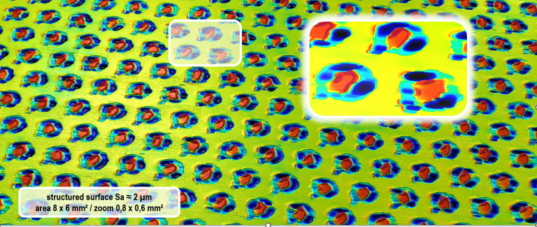
Other uses include measuring transparent coatings, evaluating cylinder bores, galvanic surfaces, or laser-structured metals. Large objects can also be reliably analyzed with portal measurement systems, where granite portals minimize thermal drift.
Practical Examples
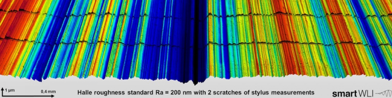
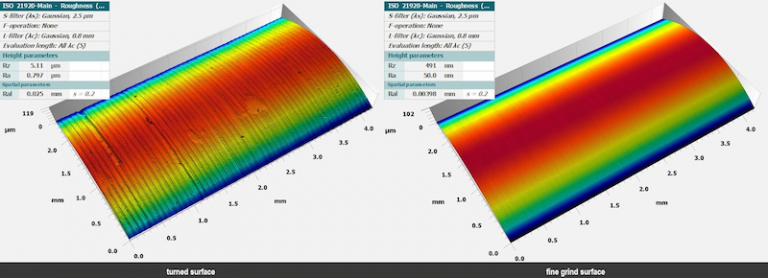
In the field of subtractive manufacturing, optical 3D sensors are used to monitor surface roughness values according to ISO EN 21920. When measuring wafers, devices such as the smartWLI firebolt8 provide precise height profiles in the sub-nanometer range.
In additive manufacturing, the smartWLI firebolt with a 5× objective enables rapid detection of surface defects on large 3D-printed components. For the analysis of diamond tools, specialized evaluation algorithms are used to determine grain density and chipping. In medical technology, implant surfaces are measured according to specific roughness values, allowing targeted influence on cell adhesion.
Integration and Automation
The integration of 3D sensors into automated production lines is supported by SDKs with C++ and C# libraries. Incorporation into existing production environments is made easy through various interfaces and customizable software solutions such as smartVIS3D and MountainsMap®. Motorized objective turrets and automated positioning systems allow flexible adaptation to different measurement tasks.
Future Trends and Innovations
Artificial intelligence and machine learning support the analysis of large datasets from 3D measurements. Sensor miniaturization enables use in confined spaces. Industry 4.0 and Smart Factory applications benefit from rapid real-time processing and transmission of measurement data. New sensor technologies and algorithms expand the range of applications, for example in measuring transparent coatings or steeply angled surfaces.
Premium Measurement Technology from GBS
Harness the full potential of state-of-the-art 3D sensors for your manufacturing, research, or quality control processes. GBS metrology GmbH offers personalized consultation, free test measurements, and tailored solutions for your measurement tasks. Benefit from our extensive experience and innovative sensor technology – from integration to practical application.
FAQ
Optical 3D sensors are suitable for a wide range of surfaces, from rough, machined metals to polished and transparent materials. Micro- and nanostructures can also be reliably captured.
Measurement times typically range from 1 to 3 seconds per single scan, depending on the application and desired resolution. This enables fast inline inspection in production processes.
Yes, integration is straightforward thanks to flexible interfaces, software SDKs, and modular design. Motorized components and customizable software support full automation.
Discover more news about GBS
Optical profilometry has advanced rapidly in recent years. While it was once primarily evaluated by how well it…
Read more