

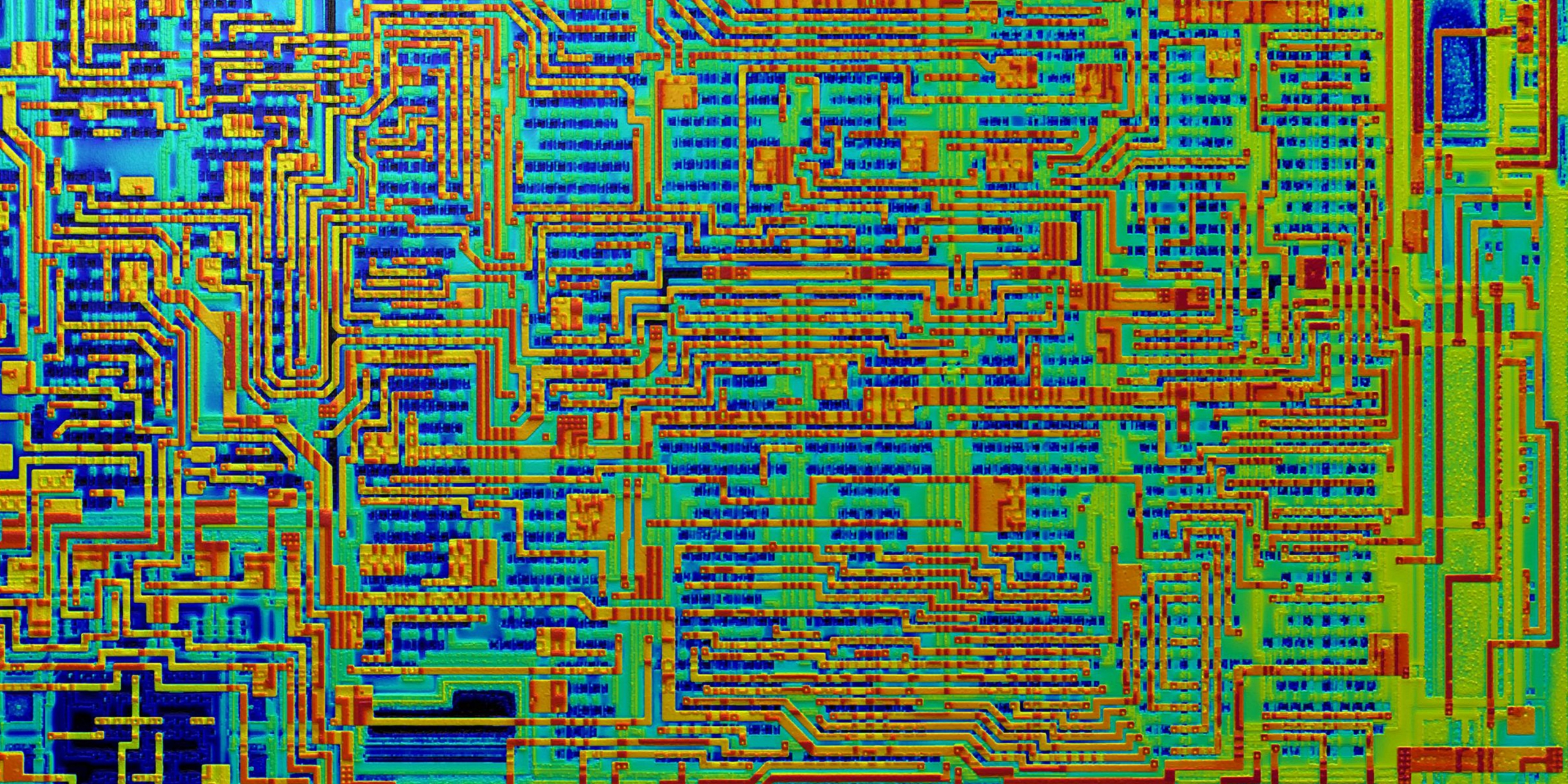
Wafer Metrology
Wafers ultimately have very smooth surfaces, so high-resolution sensors based on coherence scanning (white light) interferometry with piezo are used for corresponding measurement tasks. While sensors with just one lens (smartWLI compact, smartWLI firebolt) are used in inline monitoring of individual processes, automatic wafer measuring stations are typically equipped with sensors such as the smartWLI next and smartWLI firebolt. These sensors can be equipped with different lenses and used for different measurement tasks.
Don’t measure just anything. Measure what matters.
You can download a different number of files. Select one or more files to download.
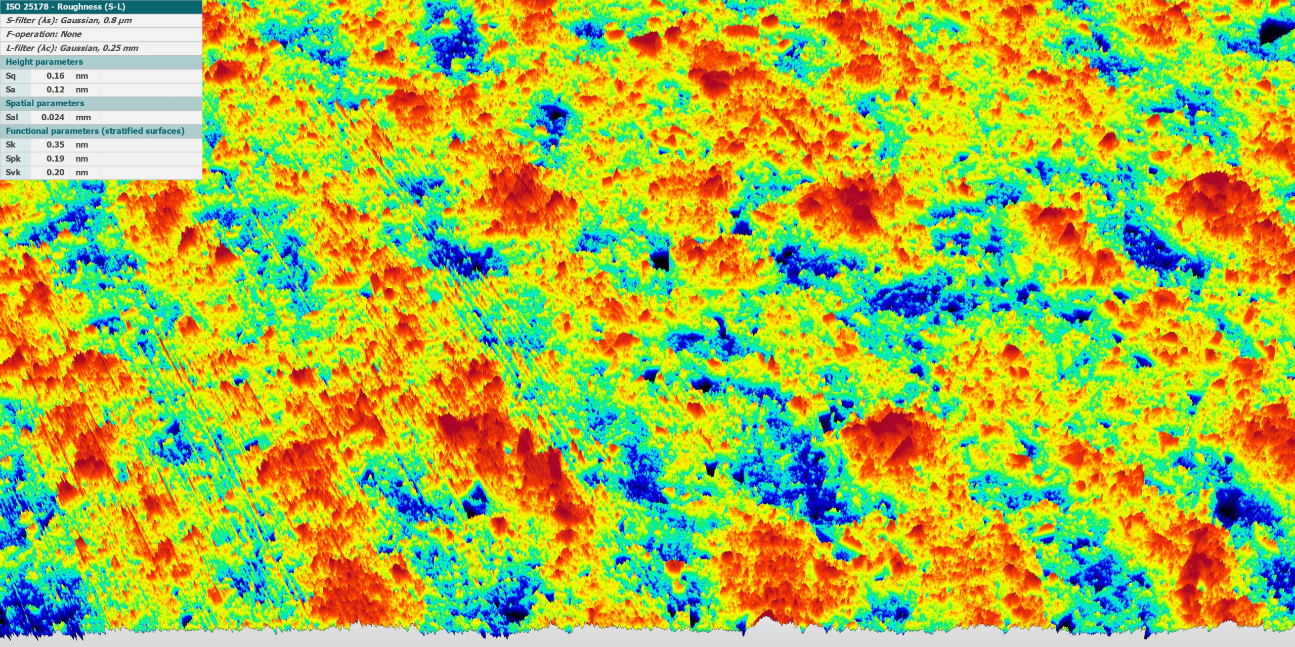
The measurement results for such surfaces demonstrate the outstanding resolution capabilities of the smartWLI series. Even with height differences in the range of an atomic diameter (1 angstrom ≙ diameter of a hydrogen atom ≙ 0.1 nm), surface structures can be clearly displayed, many measurements can be joined together without offset using smartSTITCH, and machining errors such as small scratches and dominant waviness can be clearly displayed and evaluated. Ground surfaces are relatively rough. This means that it is sufficient to use less expensive sensors without piezo positioners. For the measurements, 20x or 50x objectives should be used in order to achieve the necessary resolution for measuring finely structured surfaces.
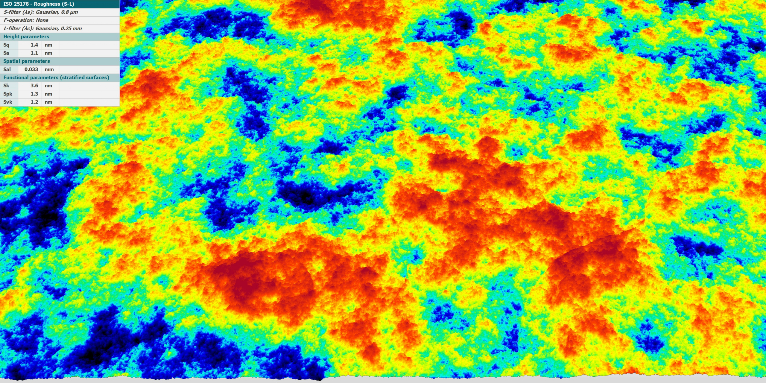
The polished wafer has locally very finely structured surface structures on the one hand, but also exhibits micro-waviness on the other. Both properties are functionally relevant, so that high-resolution measurement, e.g. with a 50x objective, should be used for quality control, for example, with a 5x objective for measuring larger areas.
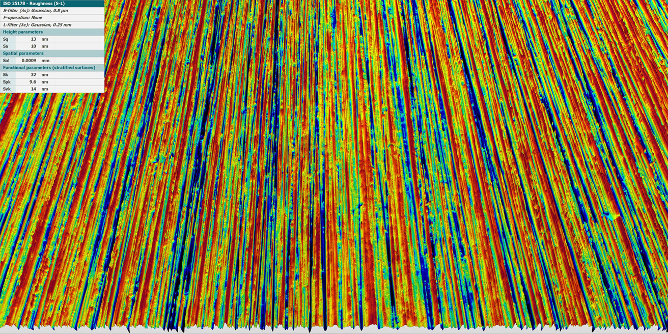
The grinded wafer has a very finely structured surface. This can be evaluated using the autocorrelation length Sal. Sal 0.9 µm means that the corresponding measuring device must also have a very high resolution. The lateral period limit DLIM (see ISO 25178-604) should be used to evaluate the structural resolution. DLIM < 0.9 is offered by the smartWLI dual and smartWLI nanoscan systems with a 50x objective. For all other systems, a 100x objective must be used for correspondingly finely structured surfaces.
Black silicon surfaces have very small structures with a very high aspect ratio. Such surfaces can only be measured using the smartWLI nanoscan and smartWLI dual systems with a 115x objective lens. The use of FFT-based quality control algorithms eliminates effects caused by interference and multiple reflections between structures in other optical measuring devices and coherence scanning (white light) interferometers without corresponding algorithms.
With measurement point intervals starting at 0.03 µm and a lateral period limit DLIM< 0.5 µm, small features or test structures on wafers can be measured quickly and easily with extreme height resolution.
