Semiconductors and wafers: Precise surface measurement technology from GBS
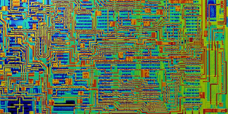
In the semiconductor industry, nanometers count—and even the smallest deviations can have a major impact. Our 3D surface measurement technology enables high-precision analysis of wafers, layers, and microstructured surfaces across all process steps.

GBS – efficient measurement systems and software solutions
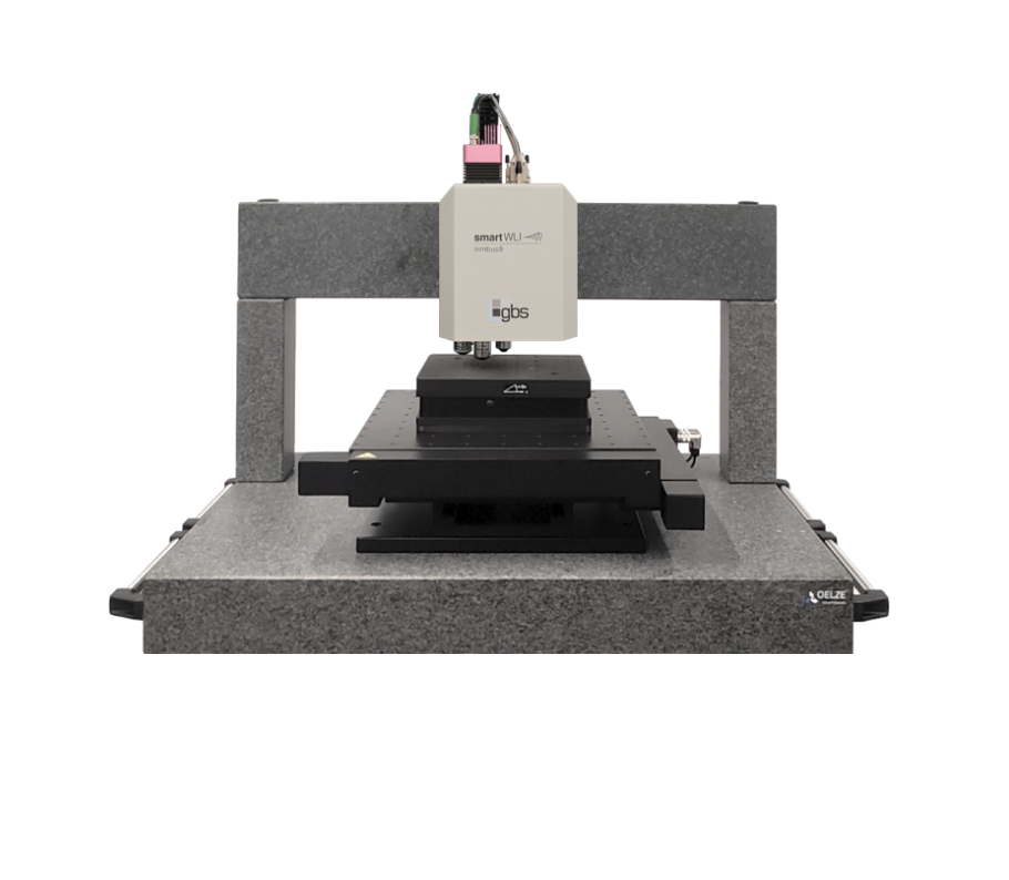
GBS metrology GmbH has been developing, manufacturing, and distributing innovative surface measurement technology for analyzing microgeometries, surface structures, and roughness since 1997. Its product range includes optical 3D sensors, profilometers, gantry measuring machines, and production-oriented measuring stations.
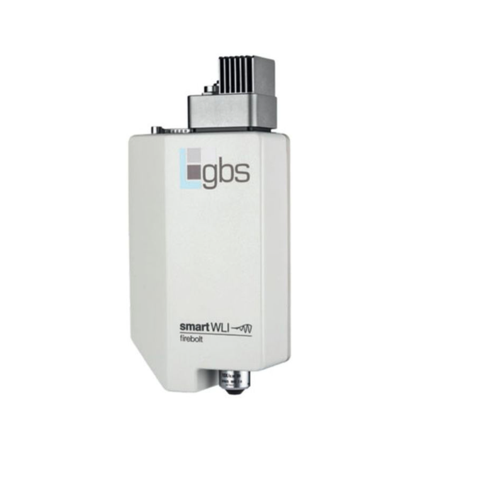
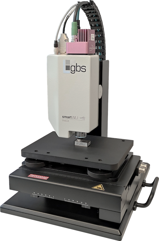
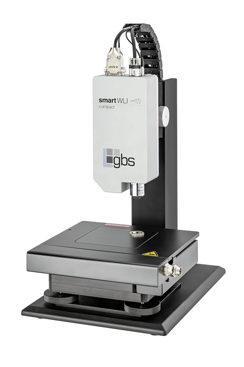
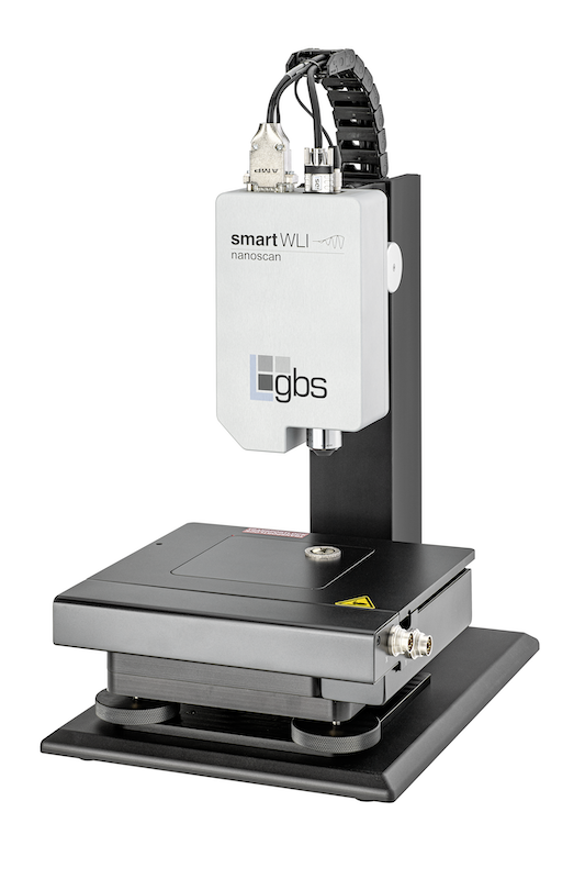
Thanks to massive parallel image processing on powerful GPGPUs, measuring devices and sensors can be used both in the laboratory and inline in production. The white light interferometry used enables extremely high resolution when capturing a wide variety of surfaces. The “smartWLI” product line stands for 3D surface measurement technology at the micro and nanostructure level.
3D surface measurement technology for semiconductors and wafers: Components and applications
Wafer manufacturing
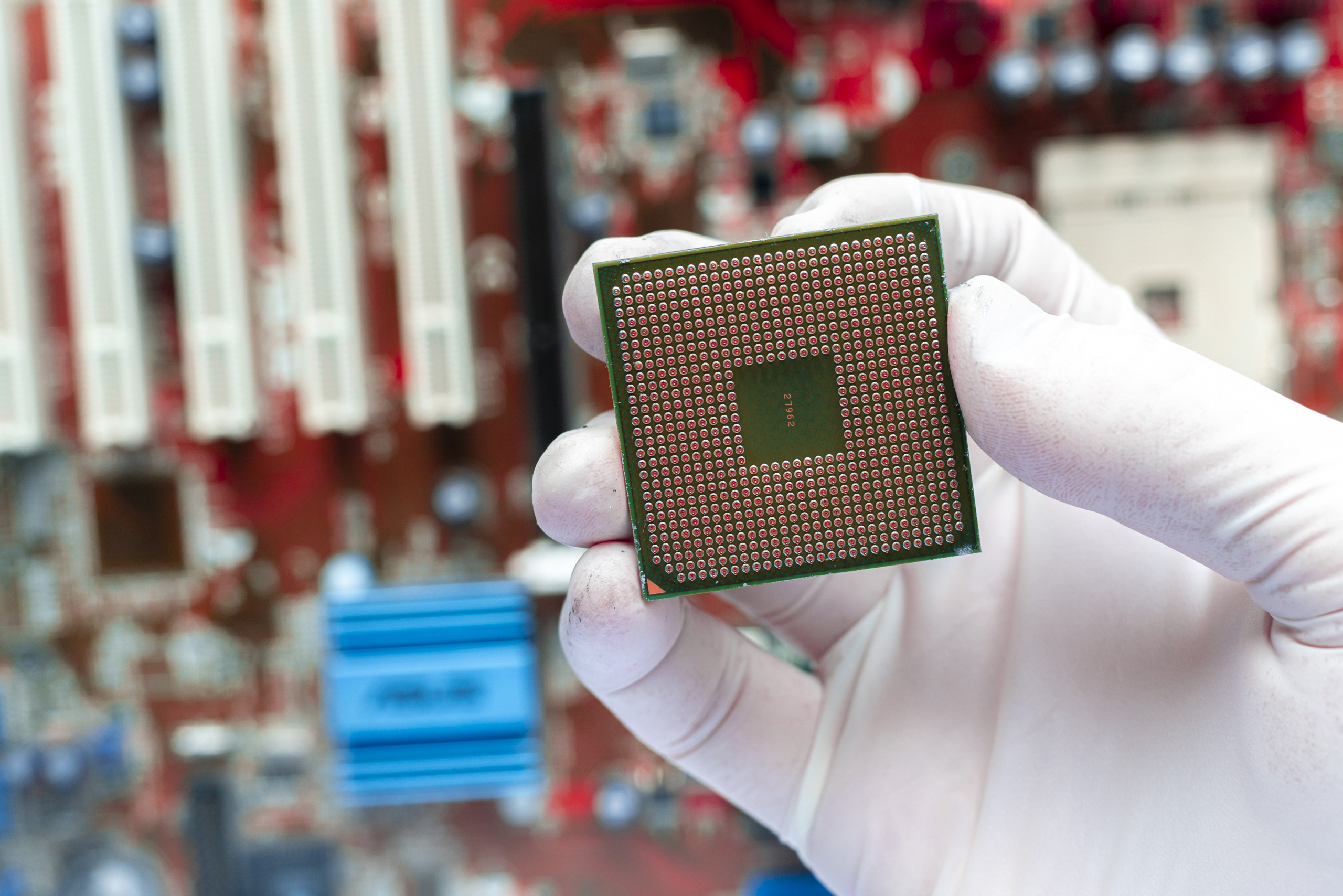
Wafers made of silicon or other semiconductor materials form the basis of microelectronic components. 3D surface metrology checks topography and flatness to ensure the basis for subsequent manufacturing processes.
Layer inspection
Thin layers and multilayers are applied during doping, etching, and coating. The measuring systems record layer thickness and surface quality without contact and detect even the smallest deviations in the nanometer and subnanometer range.
Defect detection
Structures such as scratches, particles, or local height deviations on wafers affect the reliability of components. GBS’s 3D surface measurement technology identifies defects at an early stage and provides reproducible data for error analysis.
Process control in manufacturing
Inline measuring systems continuously monitor surface quality throughout the entire production process. This keeps yields stable and production errors are detected immediately.
Quality inspection of microstructured surfaces
Micro- and nanostructures on semiconductor wafers, such as conductor tracks or contact surfaces, are inspected for roughness and geometry. The measuring systems support compliance with manufacturing tolerances.
Final inspection of semiconductor components
Before further processing or delivery, wafers and semiconductor components undergo a final inspection. 3D surface measurement technology documents all relevant parameters for quality assurance.
Technological features of our 3D surface measurement technology
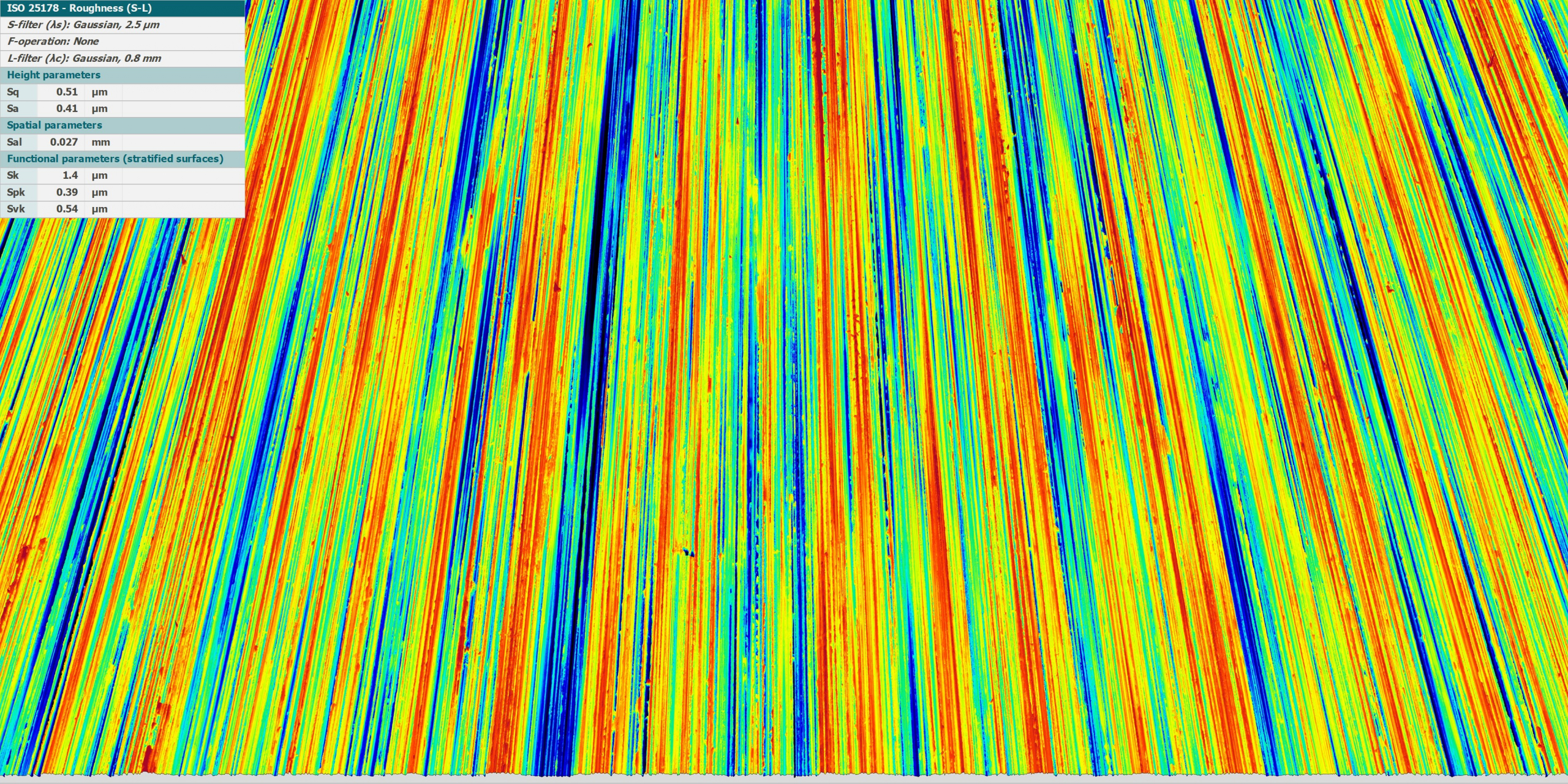
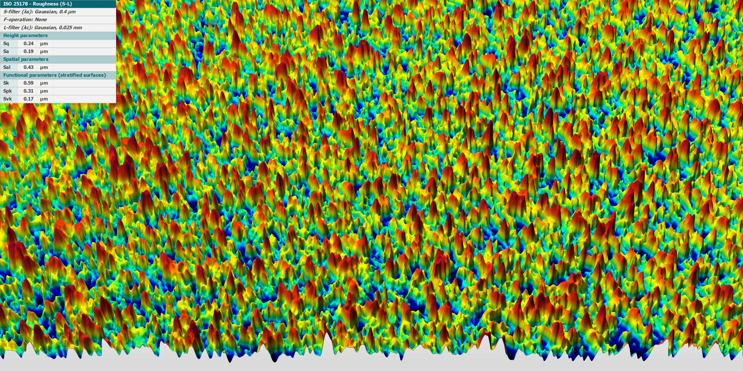
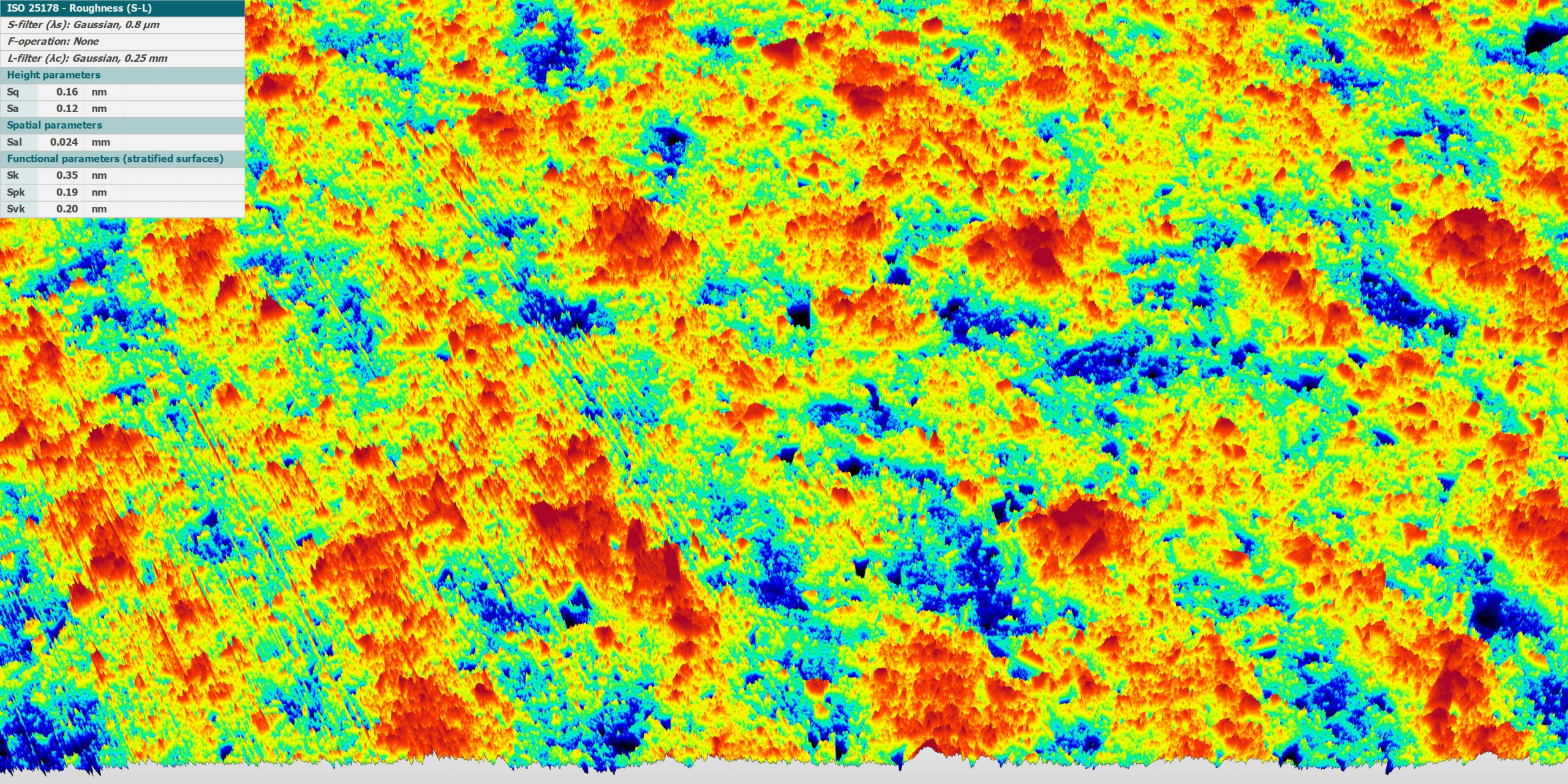
3D surface measurement technology for semiconductors and wafers uses non-contact measurement systems to inspect surface structures and layers. Unlike tactile methods, data is collected without mechanical contact, so even sensitive wafers are not damaged.
High-resolution measurements are based on methods such as white light interferometry and deliver both lateral and vertical precision. Our measurement systems combine this technology with high-speed cameras and GPU-based data processing, enabling large amounts of data to be evaluated in a short time.
Automated image analysis supports the reliable detection of topography, flatness, roughness, and defects on wafers. Even difficult surface profiles and very smooth layers can be examined in detail and reproducibly, ensuring effective process monitoring.
Advantages of 3D surface metrology for semiconductors and wafers
- Non-contact measurement protects sensitive wafer structures
- High lateral and vertical resolution for precise analyses
- Fast data processing thanks to GPU technology
- Reliable defect detection and error analysis
- Reproducible measurement data for quality assurance
- Inline integration into manufacturing processes possible
- Analysis of topography, flatness, roughness, and layers
- Suitable for micro- and nanostructures
Precise measurement technology for semiconductors and wafers
GBS offers powerful 3D surface measurement technology for high-resolution analysis of wafers, layers, and microstructured surfaces. The non-contact measurement systems capture detailed and reproducible data for process control and quality assurance in semiconductor manufacturing. With fast data acquisition and the option of inline integration, GBS increases the efficiency and reliability of your production.
Automation and integration into the production
Measuring tasks can be automated by integrating the measuring systems into production environments. Fast data acquisition enables continuous production monitoring without interrupting manufacturing.
Automated measuring stations are designed for series production and enable high yields. The measurement data provides a basis for quality control. By analyzing the measurement results, sources of error can be specifically identified and eliminated.
Documentation and traceability are part of the process. The data is archived and available for later analysis. The quality of the semiconductors and wafers remains at a consistent level.
Our product highlights


What our customers say
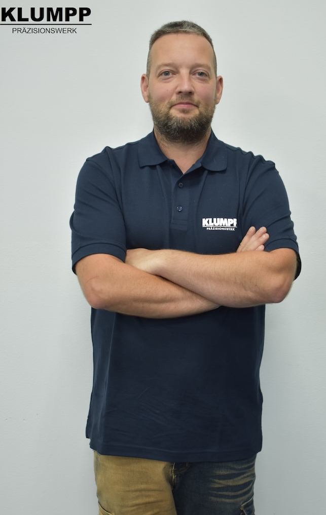
Measuring stations for rapid testing of precision turned parts in the production environment
At the start of each shift, the dimensional accuracy of the turning tools is checked in the precision turned parts production department at Klumpp Präzisionswerk GmbH & Co. KG. To this end, workpieces from ongoing production are sent to the measuring laboratory to obtain approval for further production. In series production with multiple automatic lathes, however, the large number of measurements often leads to the laboratory becoming overloaded.
GBS metrology GmbH developed an automated measuring station. The measuring station can be installed directly in the production environment, close to the lathes. This allows workers to check their finished products themselves without any prior knowledge of measurement technology or training.
After installing the measuring station from GBS metrology, it was quickly integrated into the production process and was very well received. The reduction in personnel required in the measuring laboratory and the resulting acceleration of production approval led to a clear increase in the scope and efficiency of the manufacturing processes.
FAQ
Analysis at the nanometer level allows even the smallest surface deviations to be detected at an early stage. This keeps production processes stable and increases yield and reliability in semiconductor manufacturing.
Non-contact measurement systems measure wafers and layers without damaging the sensitive structures. They provide precise and reproducible data for process control and quality assurance.
The measuring systems are designed for inline integration and can be automatically incorporated into production lines. This enables continuous monitoring and documentation of product quality.