

3D surface metrology for those who refuse to compromise on quality
Measuring perfection. In micrometers and nanometers.
Find the right optical 3D measurement solution for your application
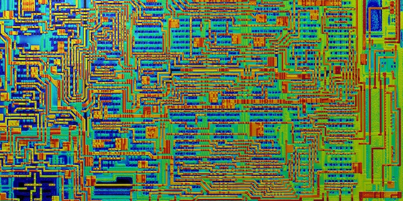
Semiconductors & Wafers

Medical technology & biomedicine
Machine & tool manufacturing

Automotive & Aerospace
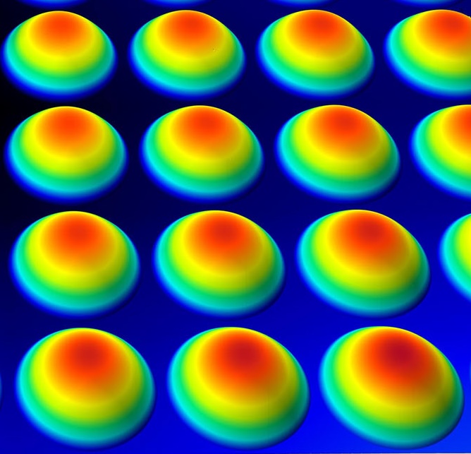
Microsystem technology
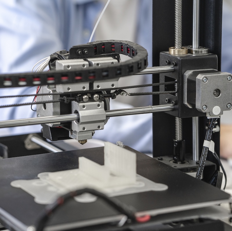
Additive manufacturing & 3D printing
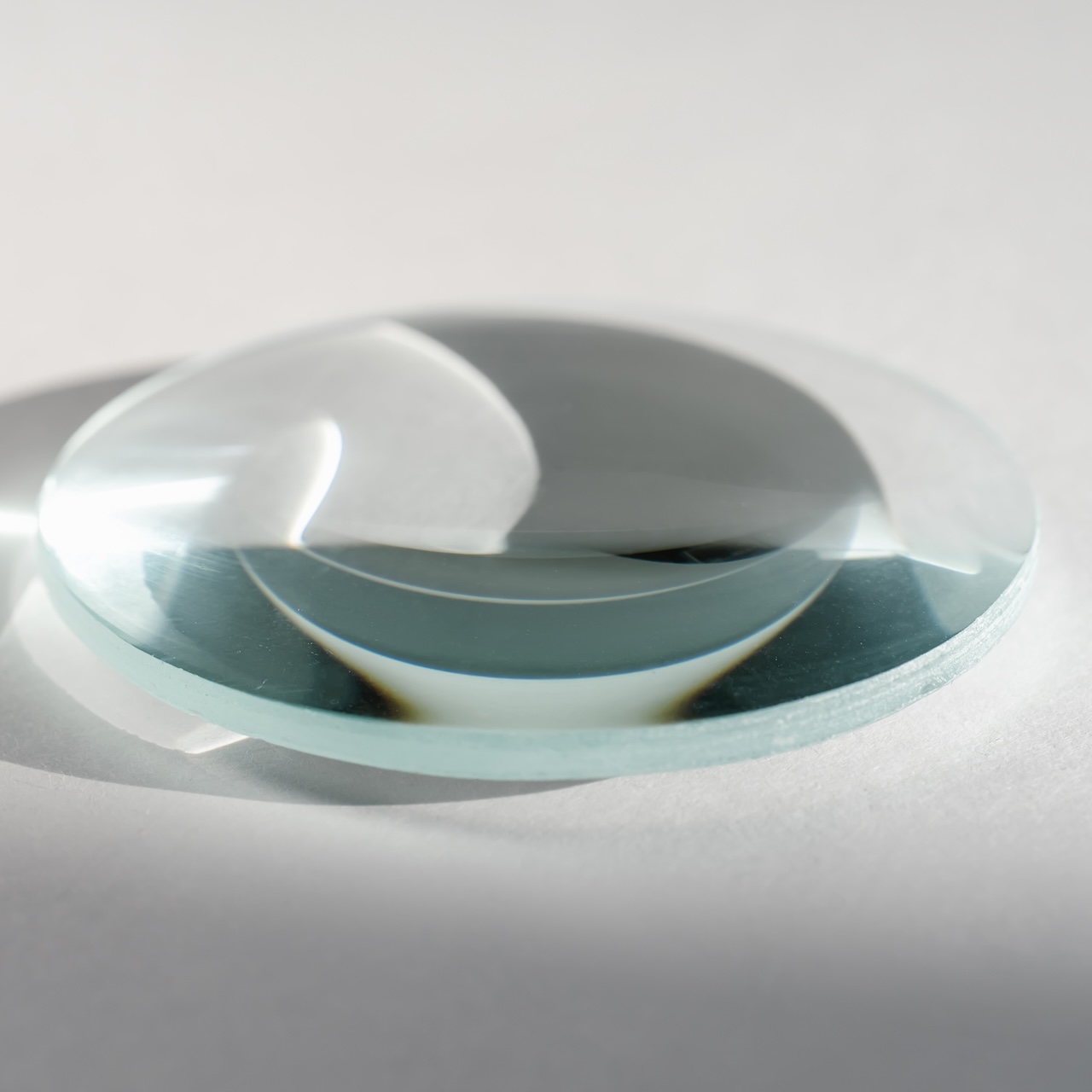
Optical components
Precise 3D surface
metrology for every application
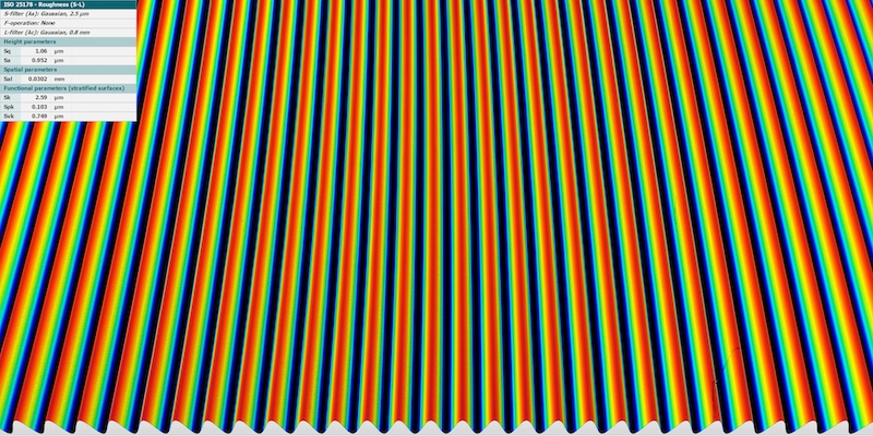
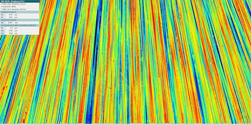
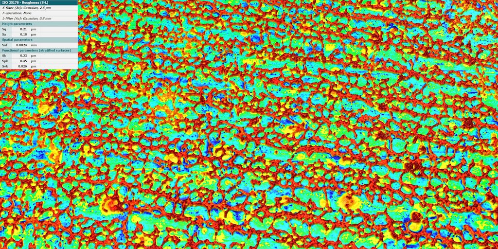
Our optical measurement solutions cover the entire spectrum of 3D surface analysis—from high-precision devices for laboratories and research to robust systems for production and integration to custom-developed special solutions. Whether you need to measure micro- and nanostructures or roughness, you will receive the optimal non-contact measurement technology for every application—reliable, flexible, and tailored precisely to your requirements.
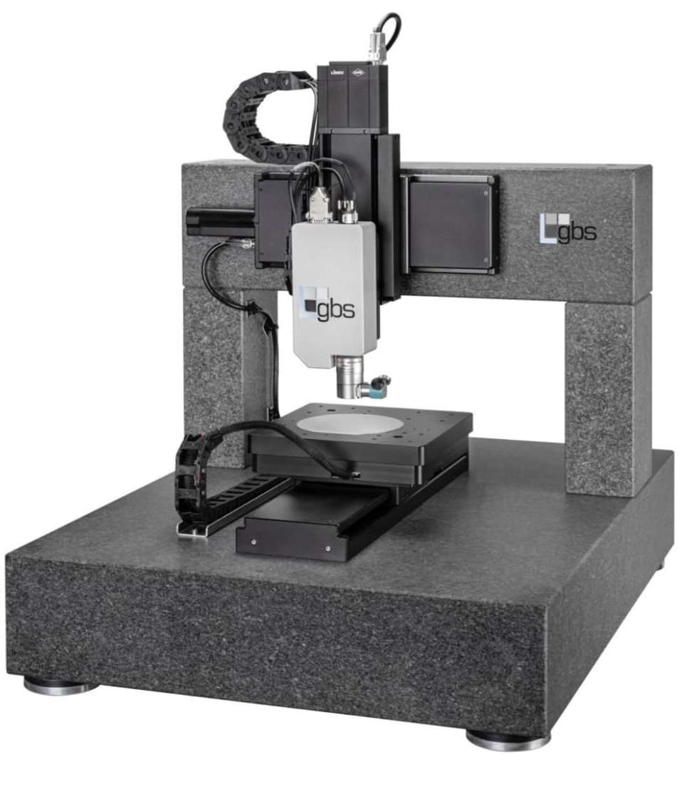
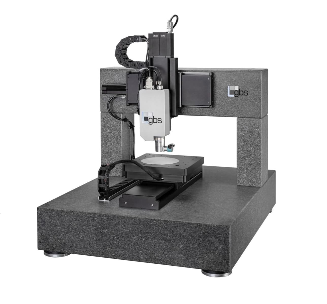
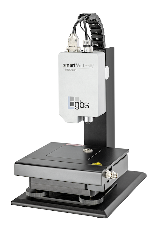
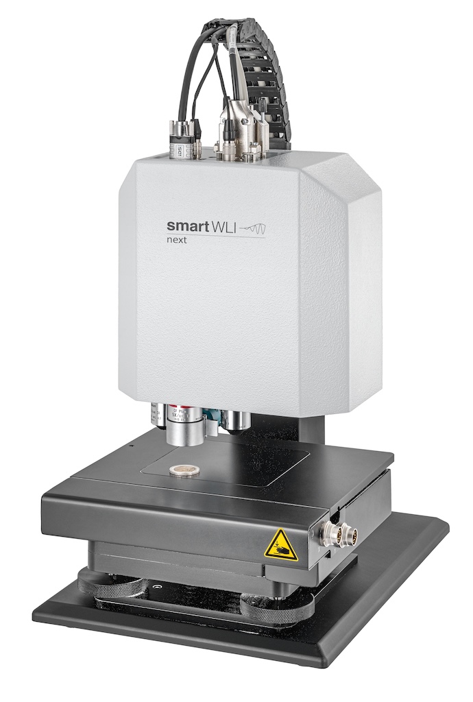
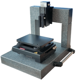
Measuring instruments for laboratory and research applications
Our measuring devices for laboratories and research are specially designed for maximum precision and flexibility. They enable detailed analyses of micro- and nanostructures and deliver reliable measurement results for demanding research and development projects. With state-of-the-art white light interferometry and innovative image processing, these systems offer ideal conditions for scientific applications and technical quality management.
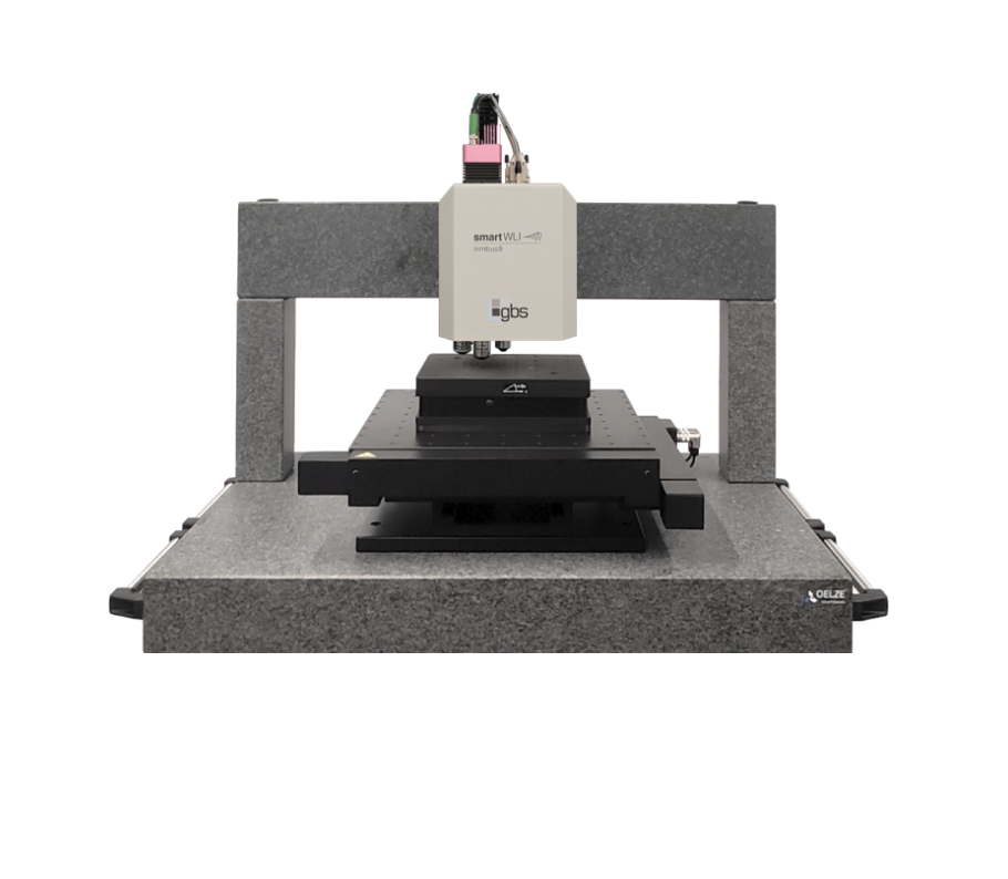
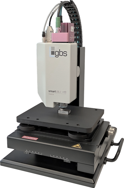
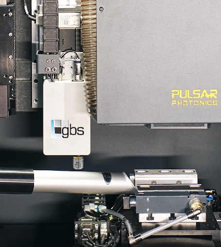
Measuring devices for the field of application Production & Integration
Designed for use in production and directly in manufacturing processes, our measuring devices are characterized by their robustness, short measuring times, and easy integration into existing production lines. They support efficient quality assurance with fast, non-contact measurements—both inline and close to production—and are specially tailored to the requirements of industrial applications.
Customized Solutions
Every product is only as good as its fit – that’s why we develop individual, customer-specific metrology solutions that are precisely tailored to your requirements and processes. Whether you need custom-made products, adaptations to existing systems, or complex measuring stations, our experienced team will support you from the design stage through to commissioning and beyond.
Why GBS?
We measure, analyze, and visualize technical surfaces in 3D—from tool steel to semiconductor wafers. Precise. Comparable. Reproducible.
Short measurement times
Real-time evaluation on GPGPUs
Nano-Precision
Measurement resolution less than 1 nm.
Ready for integration
Interfaces for every production line.
Our advantages
GBS metrology GmbH offers advanced optical 3D metrology that perfectly combines precision, reliability, and efficiency. Our non-contact systems for roughness, microstructure, and nanostructure measurements deliver reproducible results, save testing time, and can be flexibly adapted to your individual requirements—ideal for research, development, and modern manufacturing.
In-house product development
Minimal maintenance required
Full automation possible
Faster ROI of products
First-hand support
Short measurement times – real-time evaluation on GPGPUs
About us
GBS metrology GmbH was founded in 1997 and develops, manufactures, and distributes surface metrology y for recording and evaluating microgeometries, surface structures, and roughness. Our products include:
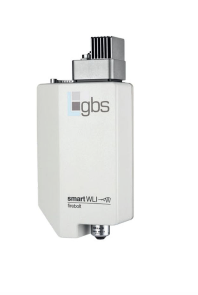
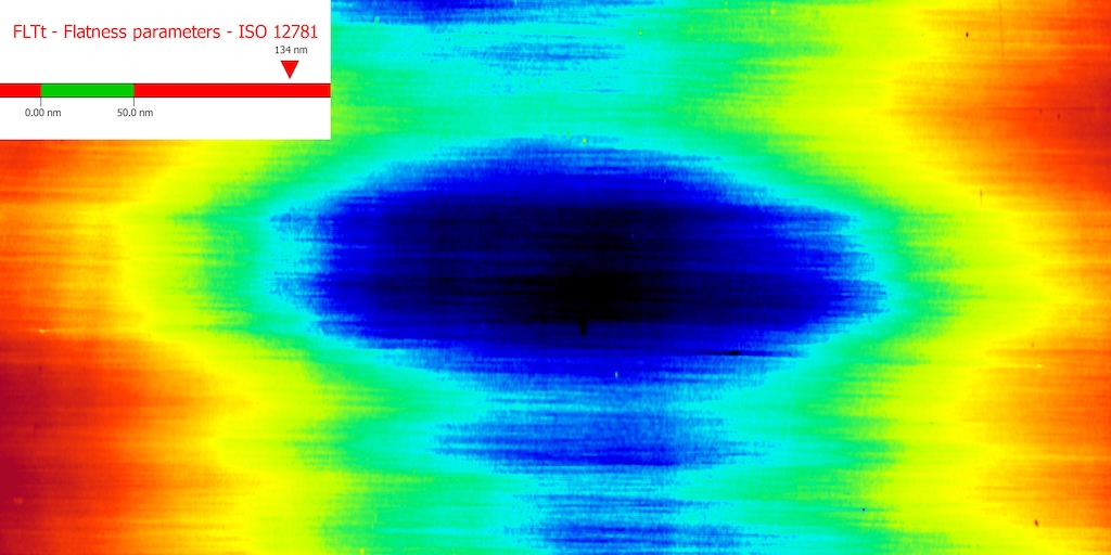
Massive parallel image processing on high-performance GPGPUs (general purpose graphic processing units) enables extremely short measurement times, allowing the measuring devices and 3D sensors to be used not only in the laboratory but also in production environments and inline. The white light interferometry (coherence scanning interferometry) measurement method used allows a wide variety of surfaces to be captured with extreme resolution.

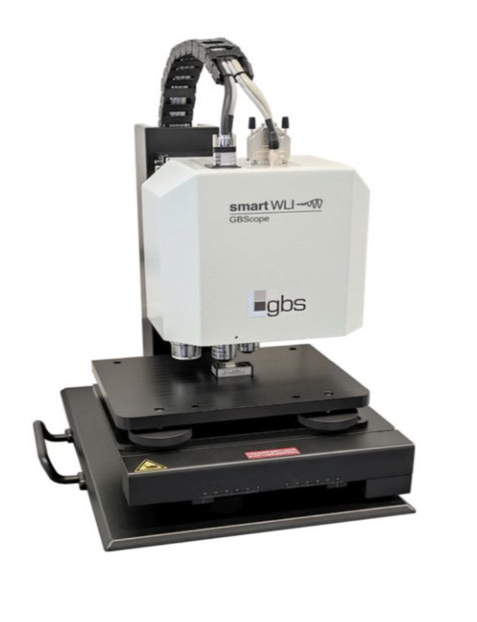
Our product highlights
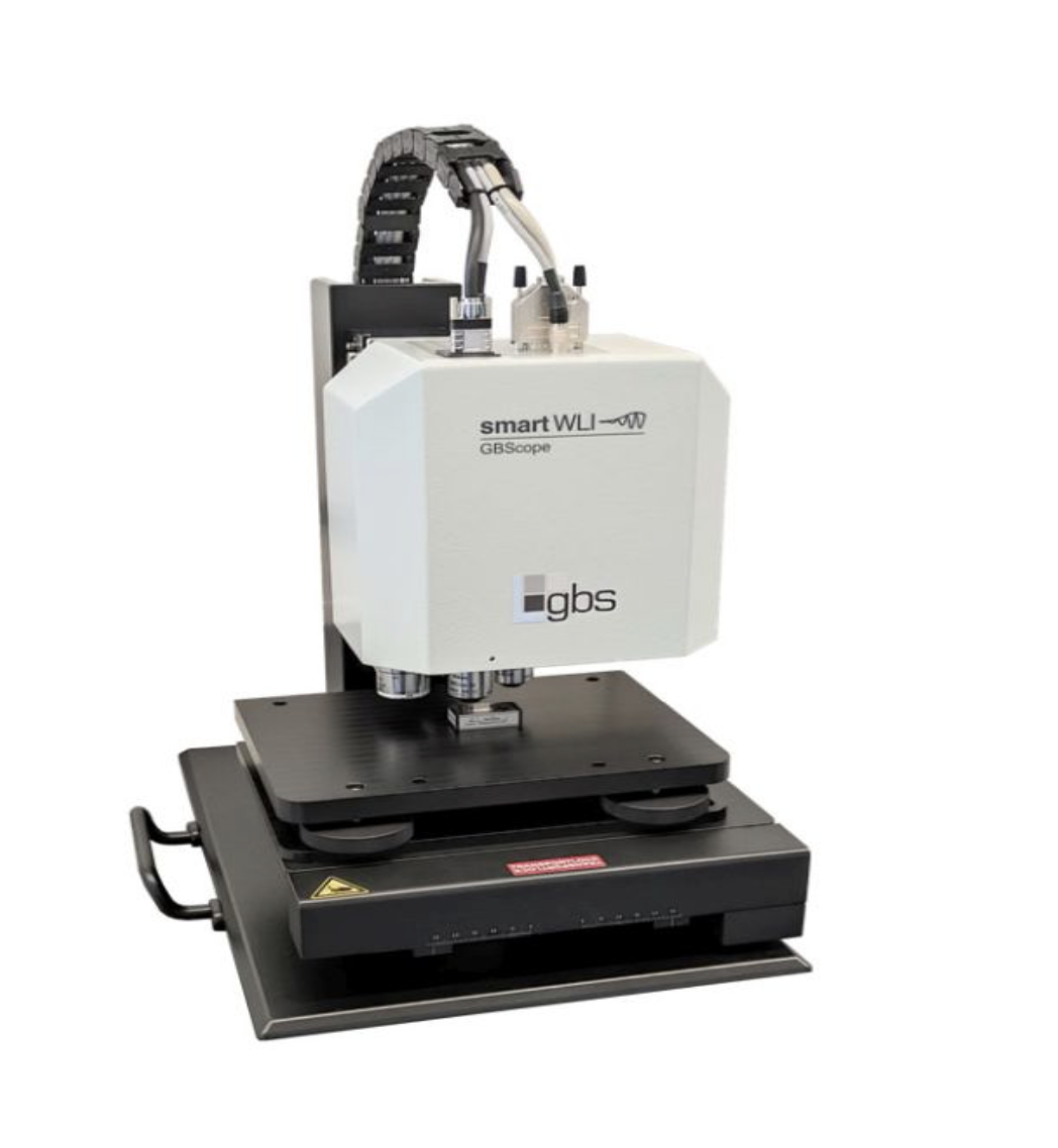
smartWLI GBScope


We offer the best solutions

(inline, automation)

What our customers say
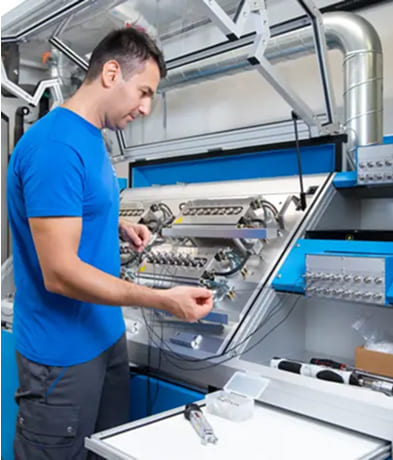
Measuring stations for rapid testing of precision turned parts in the production environment
At the start of each shift, the dimensional accuracy of the turning tools is checked in the precision turned parts production department at Klumpp Präzisionswerk GmbH & Co. KG. To this end, workpieces from ongoing production are sent to the measuring laboratory to obtain approval for further production. In series production with multiple automatic lathes, however, the large number of measurements often leads to the laboratory becoming overloaded.
GBS metrology GmbH developed an automated measuring station. The measuring station can be installed directly in the production environment, close to the lathes. This allows workers to check their finished products themselves without any prior knowledge of measurement technology or training.
After installing the measuring station from GBS metrology, it was quickly integrated into the production process and was very well received. The reduction in personnel required in the measuring laboratory and the resulting acceleration of production approval led to a clear increase in the scope and efficiency of the manufacturing processes.
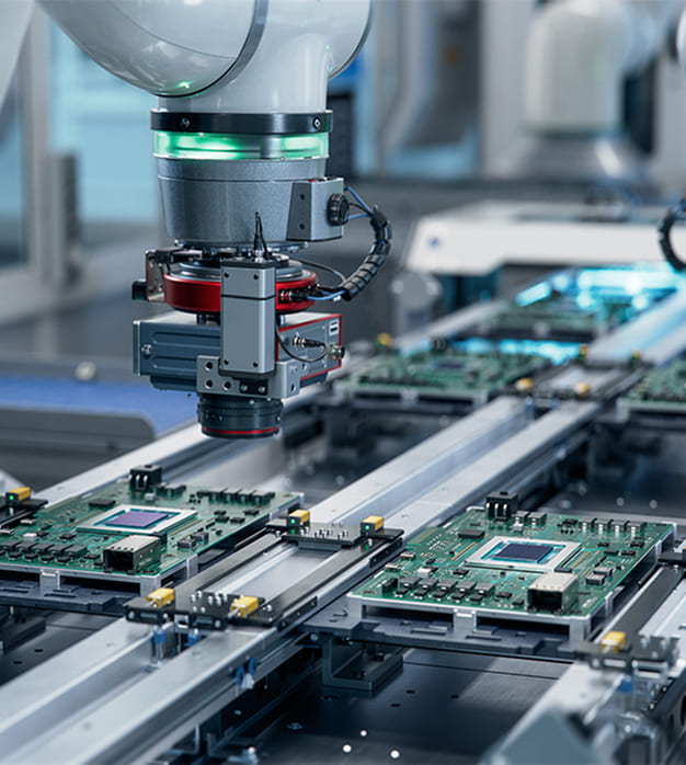
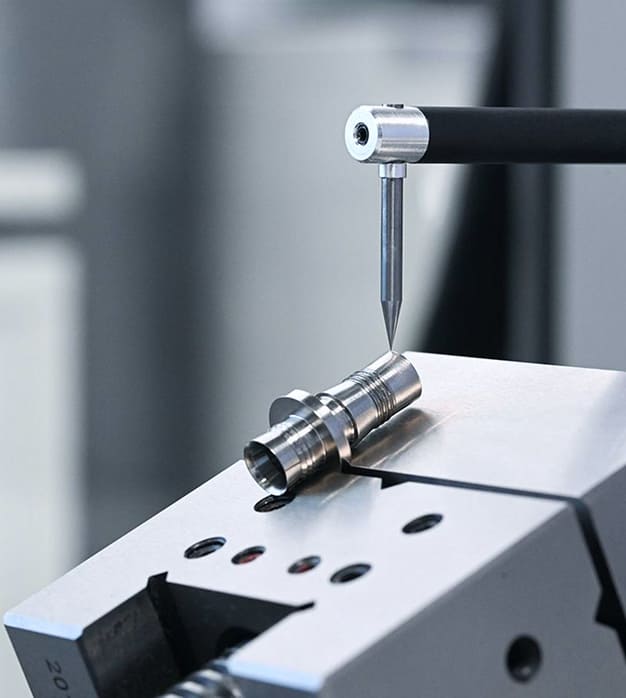
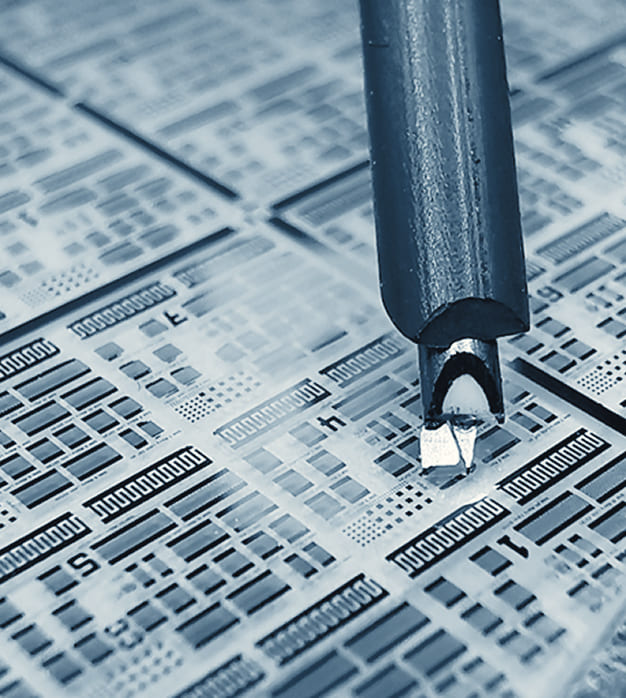
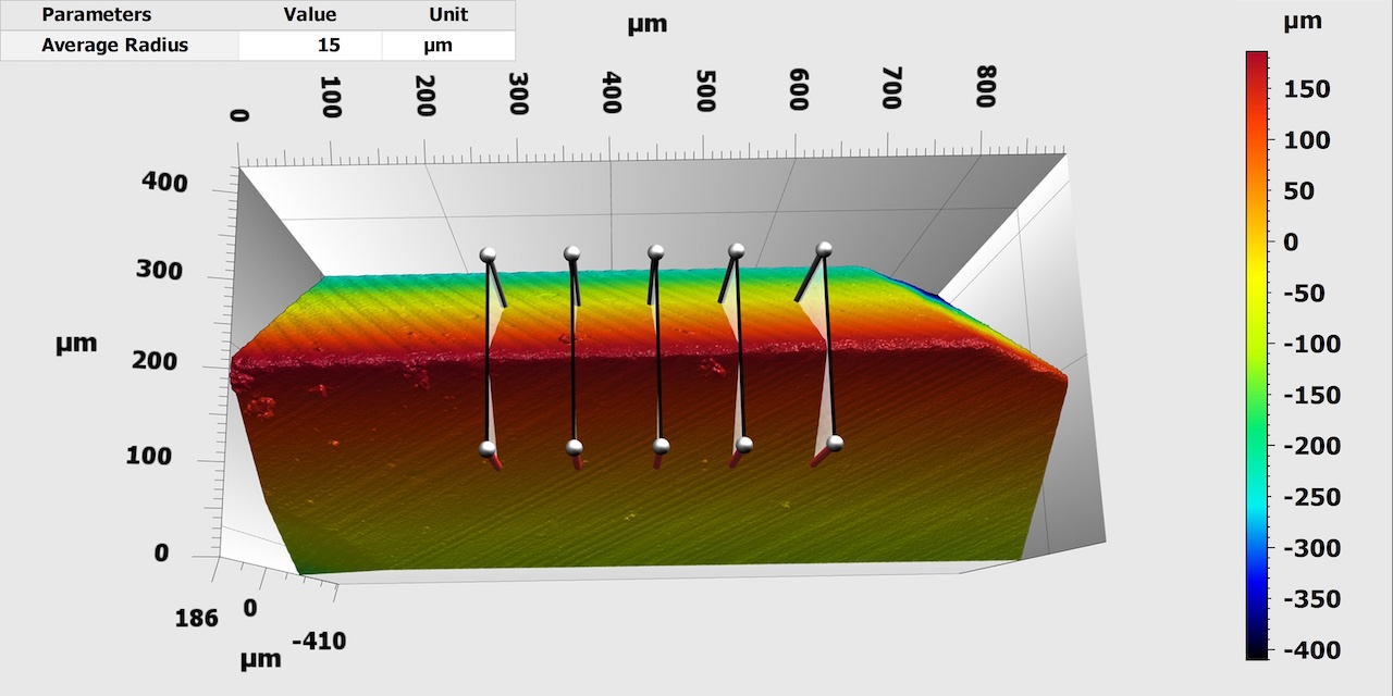
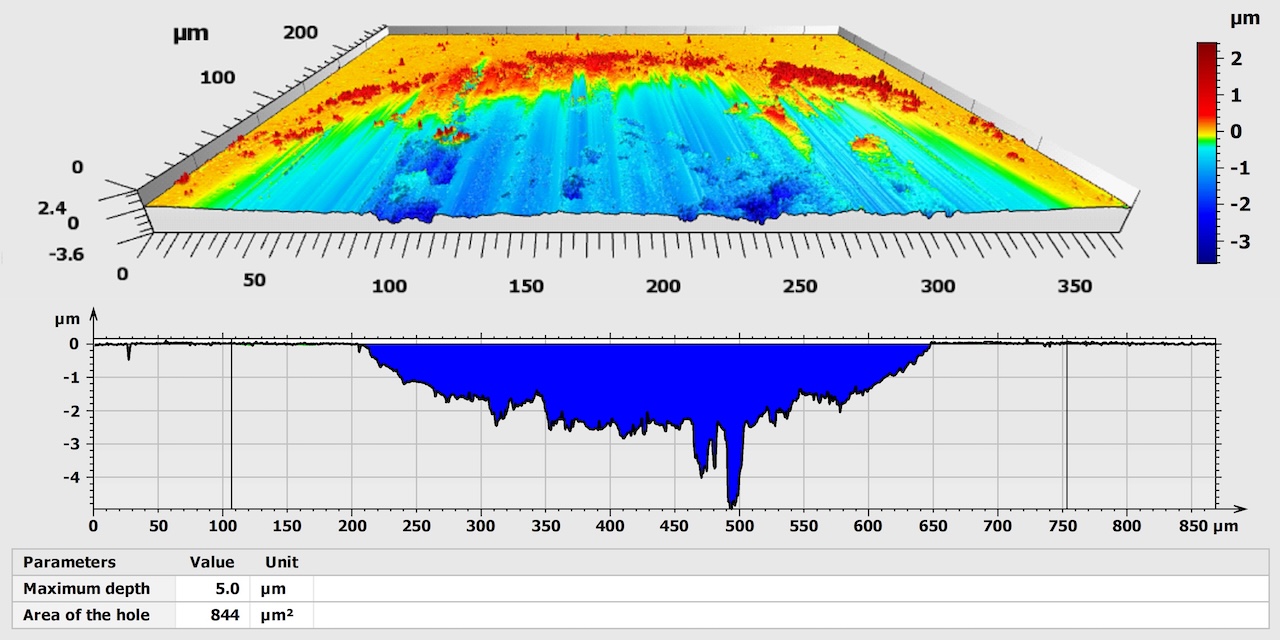
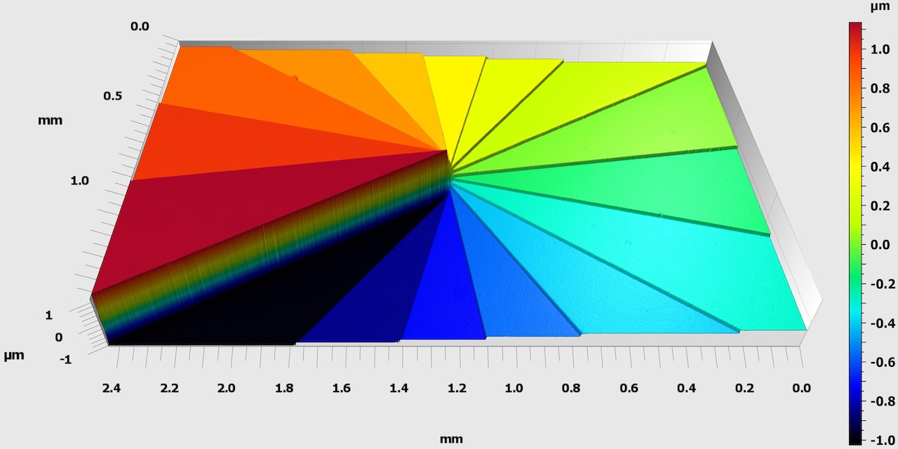
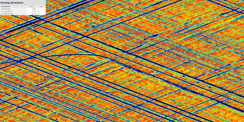
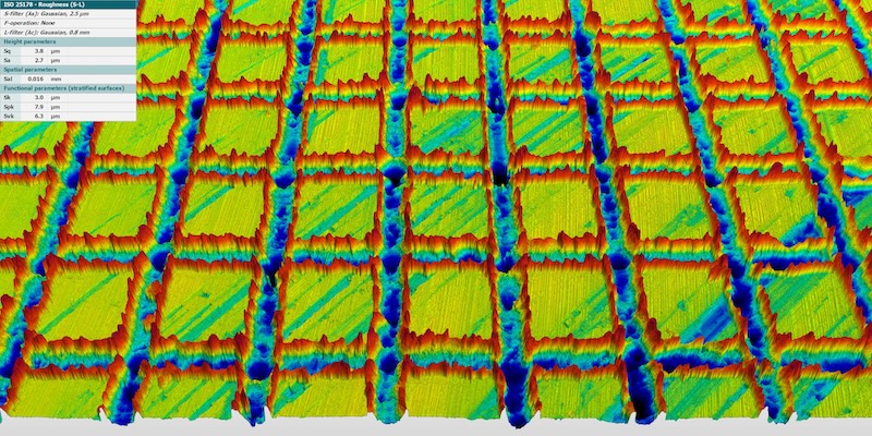
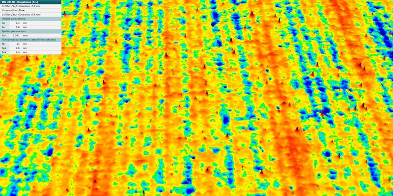
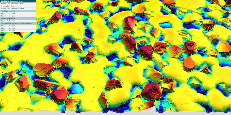
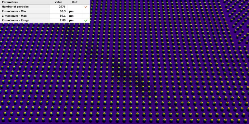
Applications in optical surface metrology
Whether machined surfaces, cutting edges, wafers, optical components, or additively manufactured structures—our systems deliver high-resolution, reliable data for a wide range of materials, geometries, and industries.
Discover how precise measurement data helps to ensure quality, optimize processes, and drive new developments—in manufacturing, in the laboratory, and beyond.


Why GBS?
We measure, analyze, and visualize technical surfaces in 3D—from tool steel to semiconductor wafers. Precise. Comparable. Reproducible.
Years of market experience
industrial partners
Made in Germany
systems installed in the last 5 years
What does the
collaboration process look like?
We accompany our customers every step of the way, from the initial idea to the final implementation. Clearly defined phases, regular coordination, and open communication ensure that projects are completed on time, to a high standard of quality, and exactly according to your requirements. Our goal: a collaborative process that builds trust and delivers sustainable results.
Initial consultation
& requirements analysis
Feasibility assessment
& proposed solution
Implementation
& Training
Ongoing support
& optimization
